ZHCSI38E March 2001 – April 2018 OPA2355 , OPA3355 , OPA355
PRODUCTION DATA.
- 1 特性
- 2 应用
- 3 说明
- 4 修订历史记录
- 5 Device Comparison Table
- 6 Pin Configuration and Functions
- 7 Specifications
- 8 Detailed Description
- 9 Application and Implementation
- 10Power Supply Recommendations
- 11Layout
- 12器件和文档支持
- 13机械、封装和可订购信息
封装选项
机械数据 (封装 | 引脚)
散热焊盘机械数据 (封装 | 引脚)
订购信息
9.2.2 High-Impedance Sensor Interface
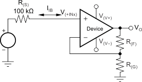
Many sensors have high source impedances that may range up to 10 MΩ, or even higher. The output signal of sensors often must be amplified or otherwise conditioned by an amplifier. The input bias current of this amplifier loads the sensor output and causes a voltage drop across the source resistance, Figure 34 shows (V(+INx) = VS – I(BIAS) × R(S).)The last term (I(BIAS) × R(S)) shows the voltage drop across R(S). To prevent errors introduced to the system as a result of this voltage, use an op amp with low input bias current with high-impedance sensors. This low current keeps the I(BIAS) × R(S) error contribution less than the input voltage noise of the amplifier so that input voltage noise is not the dominant noise factor. The OPAx355 op amps feature low input bias current (typically 200 fA), and as a result, a preferred choice for these applications.
 Figure 34. Noise as a Result of I(BIAS)