ZHCSJD6 February   2019 OPA2356-EP

PRODUCTION DATA.  

  1. 特性
  2. 应用
  3. 说明
    1.     Device Images
      1.      简化原理图
  4. 修订历史记录
  5. Pin Configuration and Functions
    1.     Pin Functions
  6. Specifications
    1. 6.1 Absolute Maximum Ratings
    2. 6.2 ESD Ratings
    3. 6.3 Recommended Operating Conditions
    4. 6.4 Thermal Information
    5. 6.5 Electrical Characteristics
    6. 6.6 Typical Characteristics
  7. Detailed Description
    1. 7.1 Overview
    2. 7.2 Functional Block Diagram
    3. 7.3 Feature Description
      1. 7.3.1 Operating Voltage
      2. 7.3.2 Output Drive
    4. 7.4 Device Functional Modes
  8. Application and Implementation
    1. 8.1 Application Information
    2. 8.2 Typical Applications
      1. 8.2.1 Transimpedance Amplifier
        1. 8.2.1.1 Design Requirements
        2. 8.2.1.2 Detailed Design Procedure
          1. 8.2.1.2.1 Custom Design With WEBENCH® Tools
          2. 8.2.1.2.2 OPA2356-EP Design Procedure
            1. 8.2.1.2.2.1 Optimizing the Transimpedance Circuit
        3. 8.2.1.3 Application Curve
      2. 8.2.2 High-Impedance Sensor Interface
      3. 8.2.3 Driving ADCs
      4. 8.2.4 Active Filter
  9. Power Supply Recommendations
  10. 10Layout
    1. 10.1 Layout Guidelines
    2. 10.2 Layout Example
  11. 11器件和文档支持
    1. 11.1 文档支持
      1. 11.1.1 相关文档
    2. 11.2 接收文档更新通知
    3. 11.3 社区资源
    4. 11.4 商标
    5. 11.5 静电放电警告
    6. 11.6 术语表
  12. 12机械、封装和可订购信息

封装选项

机械数据 (封装 | 引脚)
散热焊盘机械数据 (封装 | 引脚)
订购信息

OPA2356-EP Design Procedure

To achieve a maximally-flat, second-order Butterworth frequency response, the feedback pole must be set to:

Equation 1. OPA2356-EP q_fback_slos884.gif

Use Equation 2 to calculate the bandwidth.

Equation 2. OPA2356-EP q_bw_slos884.gif

For single-supply applications, the +INx input can be biased with a positive DC voltage to allow the output to reach true zero when the photodiode is not exposed to any light, and respond without the added delay that results from coming out of the negative rail; this configuration is shown in Figure 31. This bias voltage appears across the photodiode, providing a reverse bias for faster operation.
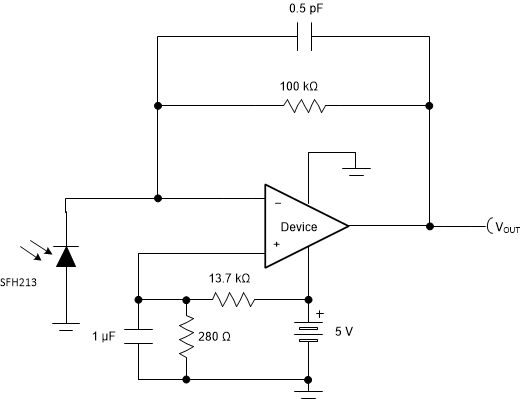
OPA2356-EP ai_trans_amp_single_sbos212.gifFigure 31. Single-Supply Transimpedance Amplifier

For additional information, see the Compensate transimpedance amplifiers intuitively application report.