ZHCSHU3A March 2018 – January 2021 OPA197-Q1 , OPA2197-Q1 , OPA4197-Q1
PRODUCTION DATA
- 1 特性
- 2 应用
- 3 说明
- 4 Revision History
- 5 Pin Configuration and Functions
-
6 Specifications
- 6.1 Absolute Maximum Ratings
- 6.2 ESD Ratings
- 6.3 Recommended Operating Conditions
- 6.4 Thermal Information: OPA197-Q1
- 6.5 Thermal Information: OPA2197-Q1
- 6.6 Thermal Information: OPA4197-Q1
- 6.7 Electrical Characteristics: VS = ±4 V to ±18 V (VS = 8 V to 36 V)
- 6.8 Electrical Characteristics: VS = ±2.25 V to ±4 V (VS = 4.5 V to 8 V)
- 6.9 Typical Characteristics
- 7 Detailed Description
- 8 Application and Implementation
- 9 Power Supply Recommendations
- 10Layout
- 11Device and Documentation Support
- 12Mechanical, Packaging, and Orderable Information
8.2.2 Slew-Rate Limit for Input Protection
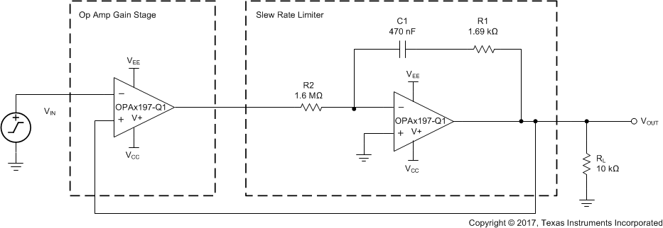
In control systems for valves or motors, abrupt changes in voltages or currents can cause mechanical damages. By controlling the slew rate of the command voltages into the drive circuits, the load voltages ramps up and down at a safe rate. For symmetrical slew-rate applications (positive slew rate equals negative slew rate), one additional op amp provides slew-rate control for a given analog gain stage. The unique input protection and high output current and slew rate of the OPAx197-Q1 make these devices the optimal amplifiers to achieve slew-rate control for both dual- and single-supply systems.Figure 8-3 shows the OPAx197-Q1 in a slew-rate limit design.
 Figure 8-3 Slew-Rate Limiter Uses One Op Amp
| For step-by-step design procedure, circuit schematics, bill of materials, PCB files, simulation results, and test results, see TI Precision Design TIPD140, Slew Rate Limiter Uses One Op Amp. | |