SBOS850 December 2017 OPA192-Q1 , OPA2192-Q1
PRODUCTION DATA.
- 1 Features
- 2 Applications
- 3 Description
- 4 Revision History
- 5 Pin Configuration and Functions
-
6 Specifications
- 6.1 Absolute Maximum Ratings
- 6.2 ESD Ratings
- 6.3 Recommended Operating Conditions
- 6.4 Thermal Information: OPA192-Q1
- 6.5 Thermal Information: OPA2192-Q1
- 6.6 Electrical Characteristics: VS = ±4 V to ±18 V (VS = 8 V to 36 V)
- 6.7 Electrical Characteristics: VS = ±2.25 V to ±4 V (VS = 4.5 V to 8 V)
- 6.8 Typical Characteristics
- 6.9 Typical Characteristics
- 7 Parameter Measurement Information
- 8 Detailed Description
- 9 Application and Implementation
- 10Power-Supply Recommendations
- 11Layout
- 12Device and Documentation Support
- 13Mechanical, Packaging, and Orderable Information
6 Specifications
6.1 Absolute Maximum Ratings(1)
over operating free-air temperature range (unless otherwise noted)| MIN | MAX | UNIT | |||
|---|---|---|---|---|---|
| Supply voltage, VS = (V+) – (V–) | ±20 (40, single-supply) |
V | |||
| Signal input pins | Voltage | Common-mode | (V–) – 0.5 | (V+) + 0.5 | V |
| Differential | (V+) – (V–) + 0.2 | ||||
| Current | ±10 | mA | |||
| Output short circuit(2) | Continuous | ||||
| Latch-up per JESD78D | Class 1 | ||||
| Temperature | Operating range | –55 | 150 | °C | |
| Junction | 150 | ||||
| Storage, Tstg | –65 | 150 | |||
(1) Stresses beyond those listed under Absolute Maximum Ratings may cause permanent damage to the device. These are stress ratings only, which do not imply functional operation of the device at these or any other conditions beyond those indicated under Recommended Operating Conditions. Exposure to absolute-maximum-rated conditions for extended periods may affect device reliability.
(2) Short-circuit to ground, one amplifier per package.
6.2 ESD Ratings
| VALUE | UNIT | ||||
|---|---|---|---|---|---|
| OPA192-Q1 | |||||
| V(ESD) | Electrostatic discharge | Human body model (HBM), per AEC Q100-002(1) | ±4000 | V | |
| Charged device model (CDM), per AEC Q100-011 | ±500 | ||||
| OPA2192-Q1 | |||||
| V(ESD) | Electrostatic discharge | Human body model (HBM), per AEC Q100-002(1) | ±4000 | V | |
| Charged device model (CDM), per AEC Q100-011 | ±500 | ||||
(1) AEC Q100-002 indicates HBM stressing is done in accordance with the ANSI/ESDA/JEDEC JS-001 specification.
6.3 Recommended Operating Conditions
over operating free-air temperature range (unless otherwise noted)| MIN | NOM | MAX | UNIT | ||
|---|---|---|---|---|---|
| Supply voltage, VS = (V+) – (V–) | 4.5 (±2.25) | 36 (±18) | V | ||
| Specified temperature | –40 | +125 | °C | ||
6.4 Thermal Information: OPA192-Q1
| THERMAL METRIC(1) | OPA192-Q1 | UNIT | |
|---|---|---|---|
| DGK (VSSOP) | |||
| 8 PINS | |||
| RθJA | Junction-to-ambient thermal resistance | 180.4 | °C/W |
| RθJC(top) | Junction-to-case (top) thermal resistance | 67.9 | °C/W |
| RθJB | Junction-to-board thermal resistance | 102.1 | °C/W |
| ψJT | Junction-to-top characterization parameter | 10.4 | °C/W |
| ψJB | Junction-to-board characterization parameter | 100.3 | °C/W |
| RθJC(bot) | Junction-to-case (bottom) thermal resistance | N/A | °C/W |
(1) For more information about traditional and new thermal metrics, see the Semiconductor and IC Package Thermal Metrics application report.
6.5 Thermal Information: OPA2192-Q1
| THERMAL METRIC(1) | OPA2192-Q1 | UNIT | |
|---|---|---|---|
| DGK (VSSOP) | |||
| 8 PINS | |||
| RθJA | Junction-to-ambient thermal resistance | 158 | °C/W |
| RθJC(top) | Junction-to-case (top) thermal resistance | 48.6 | °C/W |
| RθJB | Junction-to-board thermal resistance | 78.7 | °C/W |
| ψJT | Junction-to-top characterization parameter | 3.9 | °C/W |
| ψJB | Junction-to-board characterization parameter | 77.3 | °C/W |
| RθJC(bot) | Junction-to-case (bottom) thermal resistance | N/A | °C/W |
(1) For more information about traditional and new thermal metrics, see the Semiconductor and IC Package Thermal Metrics application report.
6.6 Electrical Characteristics: VS = ±4 V to ±18 V (VS = 8 V to 36 V)
at TA = 25°C, VCM = VOUT = VS / 2, and RLOAD = 10 kΩ connected to VS / 2 (unless otherwise noted)| PARAMETER | TEST CONDITIONS | MIN | TYP | MAX | UNIT | ||
|---|---|---|---|---|---|---|---|
| OFFSET VOLTAGE | |||||||
| VOS | Input offset voltage | ±5 | ±25 | µV | |||
| TA = 0°C to 85°C | ±8 | ±50 | |||||
| TA = –40°C to 125°C | ±10 | ±75 | |||||
| VCM = (V+) – 1.5 V | ±10 | ±40 | |||||
| TA = 0°C to 85°C | ±25 | ±150 | |||||
| TA = –40°C to 125°C | ±50 | ±250 | |||||
| dVOS/dT | Input offset voltage drift | TA = 0°C to 85°C | ±0.1 | ±0.8 | µV/°C | ||
| TA = –40°C to 125°C | ±0.2 | ±1.0 | |||||
| PSRR | Power-supply rejection ratio | TA = –40°C to 125°C | ±0.3 | ±1.0 | µV/V | ||
| INPUT BIAS CURRENT | |||||||
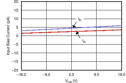
| IB | Input bias current | ±5 | ±20 | pA | |||
| TA = –40°C to 125°C | ±5 | nA | |||||
| IOS | Input offset current | ±2 | ±20 | pA | |||
| TA = –40°C to 125°C | ±2 | nA | |||||
| NOISE | |||||||
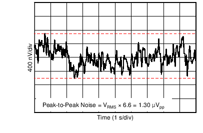
| En | Input voltage noise | (V–) – 0.1 V < VCM < (V+) – 3 V | f = 0.1 Hz to 10 Hz | 1.30 | µVPP | ||
| (V+) – 1.5 V < VCM < (V+) + 0.1 V | f = 0.1 Hz to 10 Hz | 4 | |||||
| en | Input voltage noise density | (V–) – 0.1 V < VCM < (V+) – 3 V | f = 100 Hz | 10.5 | nV/√Hz | ||
| f = 1 kHz | 5.5 | ||||||
| (V+) – 1.5 V < VCM < (V+) + 0.1 V | f = 100 Hz | 32 | |||||
| f = 1 kHz | 12.5 | ||||||
| NOISE (continued) | |||||||
| in | Input current noise density | f = 1 kHz | 1.5 | fA/√Hz | |||
| INPUT VOLTAGE | |||||||
| VCM | Common-mode voltage range | (V–) – 0.1 | (V+) + 0.1 | V | |||
| CMRR | Common-mode rejection ratio | (V–) – 0.1 V < VCM < (V+) – 3 V | 120 | 140 | dB | ||
| TA = –40°C to 125°C | 114 | 126 | |||||
| (V+) – 1.5 V < VCM < (V+) | 100 | 120 | |||||
| TA = –40°C to 125°C | 86 | 100 | |||||
| (V+) – 3 V < VCM < (V+) – 1.5 V | See Typical Characteristics | ||||||
| INPUT IMPEDANCE | |||||||
| ZID | Differential | 100 || 1.6 | MΩ || pF | ||||
| ZIC | Common-mode | 1 || 6.4 | 1013Ω || pF | ||||
| OPEN-LOOP GAIN | |||||||
| AOL | Open-loop voltage gain | (V–) + 0.6 V < VO < (V+) – 0.6 V, RLOAD = 2 kΩ | 120 | 134 | dB | ||
| TA = –40°C to 125°C | 114 | 126 | |||||
| (V–) + 0.3 V < VO < (V+) – 0.3 V, RLOAD = 10 kΩ | 126 | 140 | |||||
| TA = –40°C to 125°C | 120 | 134 | |||||
| FREQUENCY RESPONSE | |||||||
| GBW | Unity gain bandwidth | 10 | MHz | ||||
| SR | Slew rate | G = 1, 10-V step | 20 | V/µs | |||
| ts | Settling time | To 0.01% | V S = ±18 V, G = 1, 10-V step | 1.4 | µs | ||
| V S = ±18 V, G = 1, 5-V step | 0.9 | ||||||
| To 0.001% | V S = ±18 V, G = 1, 10-V step | 2.1 | |||||
| V S = ±18 V, G = 1, 5-V step | 1.8 | ||||||
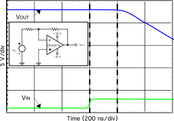
| tOR | Overload recovery time | VIN × G = VS | 200 | ns | |||
| THD+N | Total harmonic distortion + noise | G = 1, f = 1 kHz, VO = 3.5 VRMS | 0.00008% | ||||
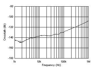
| Crosstalk | OPA2192-Q1 at dc | 150 | dB | ||||
| OPA2192-Q1 at f = 100 kHz | 130 | ||||||
| OUTPUT | |||||||
| VO | Voltage output swing from rail | Positive rail | No load | 5 | 15 | mV | |
| RLOAD = 10 kΩ | 95 | 110 | |||||
| RLOAD = 2 kΩ | 430 | 500 | |||||
| Negative rail | No load | 5 | 15 | ||||
| RLOAD = 10 kΩ | 95 | 110 | |||||
| RLOAD = 2 kΩ | 430 | 500 | |||||
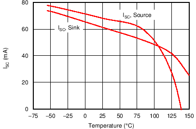
| ISC | Short-circuit current | ±65 | mA | ||||
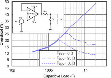
| CLOAD | Capacitive load drive | See Typical Characteristics | |||||
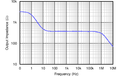
| ZO | Open-loop output impedance | f = 1 MHz, IO = 0 A; see Figure 29 | 375 | Ω | |||
| POWER SUPPLY | |||||||
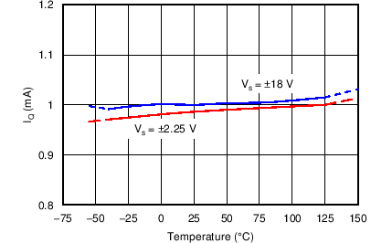
| IQ | Quiescent current per amplifier | IO = 0 A | 1 | 1.2 | mA | ||
| TA = –40°C to 125°C, IO = 0 A | 1.5 | ||||||
| TEMPERATURE | |||||||
| Thermal protection(1) | 140 | °C | |||||
6.7 Electrical Characteristics: VS = ±2.25 V to ±4 V (VS = 4.5 V to 8 V)
at TA = 25°C, VCM = VOUT = VS / 2, and RLOAD = 10 kΩ connected to VS / 2 (unless otherwise noted)| PARAMETER | TEST CONDITIONS | MIN | TYP | MAX | UNIT | ||
|---|---|---|---|---|---|---|---|
| OFFSET VOLTAGE | |||||||
| VOS | Input offset voltage | VCM = (V+) – 3 V | ±5 | ±25 | µV | ||
| TA = 0°C to 85°C | ±8 | ±50 | |||||
| TA = –40°C to 125°C | ±10 | ±75 | |||||
| (V+) – 3.5 V < VCM < (V+) – 1.5 V | See Common-Mode Voltage Range | ||||||
| VCM = (V+) – 1.5 V | ±10 | ±40 | µV | ||||
| TA = 0°C to 85°C | ±25 | ±150 | |||||
| TA = –40°C to 125°C | ±50 | ±250 | |||||
| dVOS/dT | Input offset voltage drift | VCM = (V+) – 3 V | TA = 0°C to 85°C | ±0.1 | ±0.8 | µV/°C | |
| TA = –40°C to 125°C | ±0.2 | ±1.1 | |||||
| VCM = (V+) – 1.5 V, TA = –40°C to 125°C | ±0.5 | ±3 | |||||
| PSRR | Power-supply rejection ratio | TA = –40°C to 125°C, VCM = VS / 2 – 0.75 V | ±1 | µV/V | |||
| INPUT BIAS CURRENT | |||||||
| IB | Input bias current | ±5 | ±20 | pA | |||
| TA = –40°C to 125°C | ±5 | nA | |||||
| IOS | Input offset current | ±2 | ±20 | pA | |||
| TA = –40°C to 125°C | ±2 | nA | |||||
| NOISE | |||||||
| En | Input voltage noise | (V–) – 0.1 V < VCM < (V+) – 3 V, f = 0.1 Hz to 10 Hz | 1.30 | µVPP | |||
| (V+) – 1.5 V < VCM < (V+) + 0.1 V, f = 0.1 Hz to 10 Hz | 4 | ||||||
| en | Input voltage noise density | (V–) – 0.1 V < VCM < (V+) – 3 V | f = 100 Hz | 10.5 | nV/√Hz | ||
| f = 1 kHz | 5.5 | ||||||
| (V+) – 1.5 V < VCM < (V+) + 0.1 V | f = 100 Hz | 32 | |||||
| f = 1 kHz | 12.5 | ||||||
| in | Input current noise density | f = 1 kHz | 1.5 | fA/√Hz | |||
| INPUT VOLTAGE | |||||||
| VCM | Common-mode voltage range | (V–) – 0.1 | (V+) + 0.1 | V | |||
| CMRR | Common-mode rejection ratio | (V–) – 0.1 V < VCM < (V+) – 3 V | 94 | 110 | dB | ||
| TA = –40°C to 125°C | 90 | 104 | |||||
| (V+) – 1.5 V < VCM < (V+) | 100 | 120 | |||||
| TA = –40°C to 125°C | 84 | 100 | |||||
| (V+) – 3 V < VCM < (V+) – 1.5 V | See Typical Characteristics | ||||||
| INPUT IMPEDANCE | |||||||
| ZID | Differential | 100 || 1.6 | MΩ || pF | ||||
| ZIC | Common-mode | 1 || 6.4 | 1013Ω || pF | ||||
| OPEN-LOOP GAIN | |||||||
| AOL | Open-loop voltage gain | (V–) + 0.6 V < VO < (V+) – 0.6 V, RLOAD = 2 kΩ | 110 | 120 | dB | ||
| TA = –40°C to 125°C | 100 | 114 | |||||
| (V–) + 0.3 V < VO < (V+) – 0.3 V, RLOAD = 10 kΩ | 110 | 126 | |||||
| TA = –40°C to 125°C | 110 | 120 | |||||
| FREQUENCY RESPONSE | |||||||
| GBW | Unity gain bandwidth | 10 | MHz | ||||
| SR | Slew rate | G = 1, 10-V step | 20 | V/µs | |||
| ts | Settling time | To 0.01% | VS = ±3 V, G = 1, 5-V step | 1 | µs | ||
| tOR | Overload recovery time | VIN× G = VS | 200 | ns | |||
| Crosstalk | OPA2192-Q1 at dc | 150 | dB | ||||
| OPA2192-Q1 f = 100 kHz | 130 | ||||||
| OUTPUT | |||||||
| VO | Voltage output swing from rail | Positive rail | No load | 5 | 15 | mV | |
| RLOAD = 10 kΩ | 95 | 110 | |||||
| RLOAD = 2 kΩ | 430 | 500 | |||||
| Negative rail | No load | 5 | 15 | ||||
| RLOAD = 10 kΩ | 95 | 110 | |||||
| RLOAD = 2 kΩ | 430 | 500 | |||||
| ISC | Short-circuit current | ±65 | mA | ||||
| CLOAD | Capacitive load drive | See Typical Characteristics | |||||
| ZO | Open-loop output impedance | f = 1 MHz, IO = 0 A; see Figure 29 | 375 | Ω | |||
| POWER SUPPLY | |||||||
| IQ | Quiescent current per amplifier | IO = 0 A | 1 | 1.2 | mA | ||
| TA = –40°C to 125°C | 1.5 | ||||||
| TEMPERATURE | |||||||
| Thermal protection(1) | 140 | °C | |||||
(1) For a detailed description of thermal protection, see Thermal Protection .
6.8 Typical Characteristics
Table 1. Table of Graphs
| DESCRIPTION | FIGURE |
|---|---|
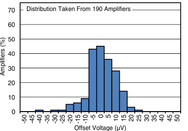
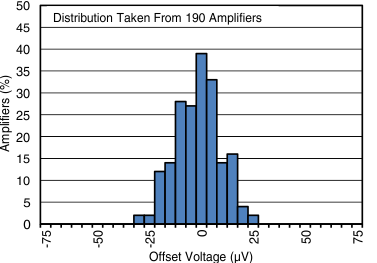
| Offset Voltage Production Distribution | Figure 1 to Figure 6 |
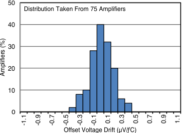
| Offset Voltage Drift Distribution | Figure 7 to Figure 8 |
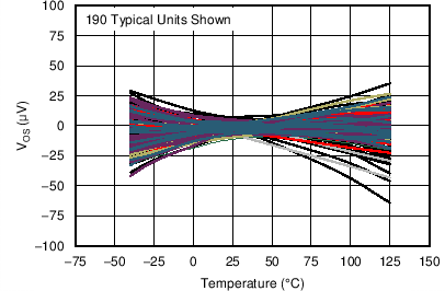
| Offset Voltage vs Temperature | Figure 9 |
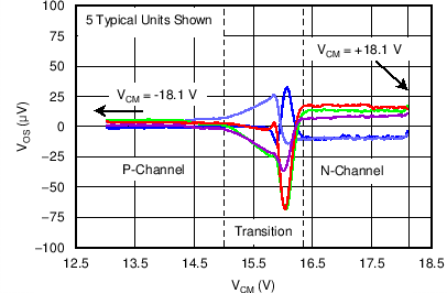
| Offset Voltage vs Common-Mode Voltage | Figure 10 to Figure 12 |
| Offset Voltage vs Power Supply | Figure 13 |
| Open-Loop Gain and Phase vs Frequency | Figure 14 |
| Closed-Loop Gain and Phase vs Frequency | Figure 15 |
| Input Bias Current vs Common-Mode Voltage | Figure 16 |
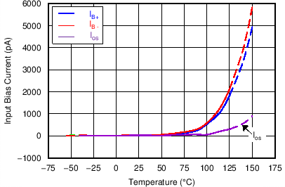
| Input Bias Current vs Temperature | Figure 17 |
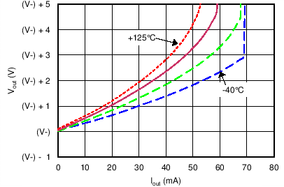
| Output Voltage Swing vs Output Current (maximum supply) | Figure 18 |
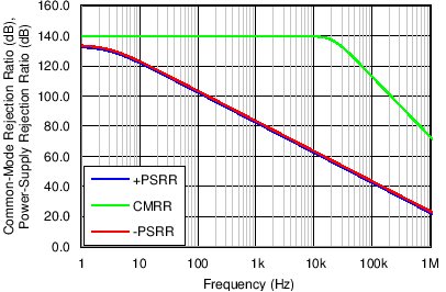
| CMRR and PSRR vs Frequency | Figure 19 |
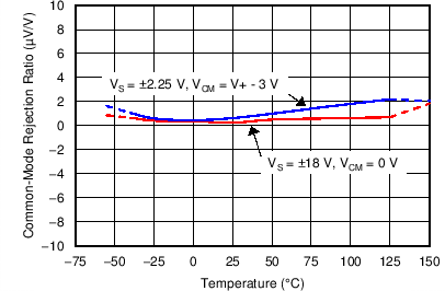
| CMRR vs Temperature | Figure 20 |
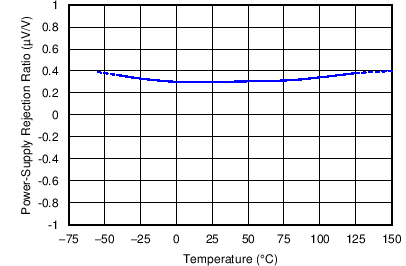
| PSRR vs Temperature | Figure 21 |
| 0.1-Hz to 10-Hz Noise | Figure 22 |
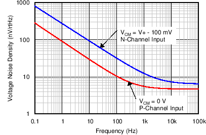
| Input Voltage Noise Spectral Density vs Frequency | Figure 23 |
| THD+N Ratio vs Frequency | Figure 24 |
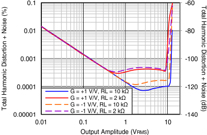
| THD+N vs Output Amplitude | Figure 25 |
| Quiescent Current vs Supply Voltage | Figure 26 |
| Quiescent Current vs Temperature | Figure 27 |
| Open Loop Gain vs Temperature | Figure 28 |
| Open Loop Output Impedance vs Frequency | Figure 29 |
| Small Signal Overshoot vs Capacitive Load (100-mV Output Step) | Figure 30, Figure 31 |
| No Phase Reversal | Figure 32 |
| Positive Overload Recovery | Figure 33 |
| Negative Overload Recovery | Figure 34 |
| Small-Signal Step Response (100 mV) | Figure 35, Figure 36 |
| Large-Signal Step Response | Figure 37 |
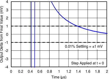
| Settling Time | Figure 38 to Figure 41 |
| Short-Circuit Current vs Temperature | Figure 42 |
| Maximum Output Voltage vs Frequency | Figure 43 |
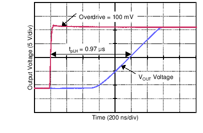
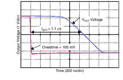
| Propagation Delay Rising Edge | Figure 44 |
| Propagation Delay Falling Edge | Figure 45 |
| Crosstalk vs Frequency | Figure 46 |
6.9 Typical Characteristics
at TA = 25°C, VS = ±18 V, VCM = VS / 2, RLOAD = 10 kΩ connected to VS / 2, and CL = 100 pF, (unless otherwise noted)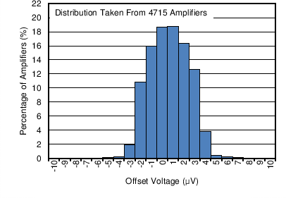
| TA = 25°C |
| TA = 85°C |
| TA = –25°C |
| OPA192-Q1IDGK and OPA2192-Q1IDGK | ||
| TA = –40°C to +125°C |
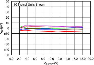
| VS = ±2.25 V to ±18 V | ||
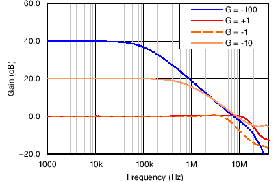
vs Frequency
| f = 1 kHz, BW = 80 kHz | ||
| G = 1 | ||
(100-mV Output Step)
| RI = 1 kΩ | RF = 10 kΩ | G = –10 |
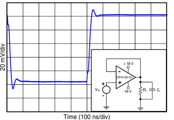
| CL = 10 pF | G = 1 | |
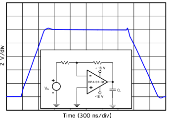
| RL = 1 kΩ | CL = 10 pF | G = –1 |
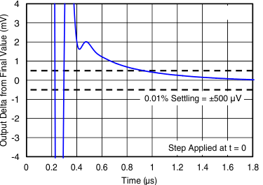
| G = 1 | ||

| G = 1 |
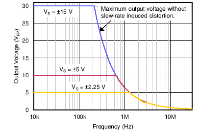
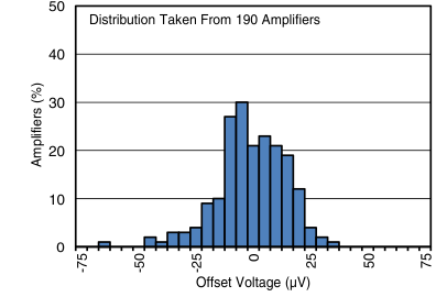
| TA = 125°C |
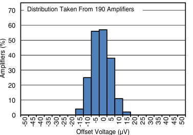
| TA = 0°C |
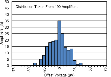
| TA = –40° C |
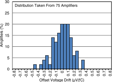
| OPA192-Q1IDGK and OPA2192-Q1IDGK | ||
| TA = 0°C to 85°C |
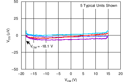
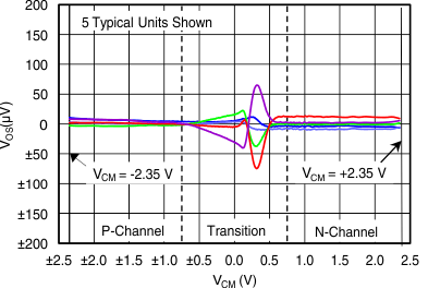
| VS = ±2.25 V | ||
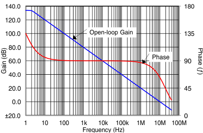
| CLOAD = 15 pF | ||
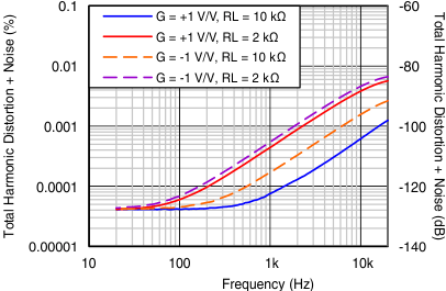
| VOUT = 3.5 VRMS | BW = 80 kHz | |
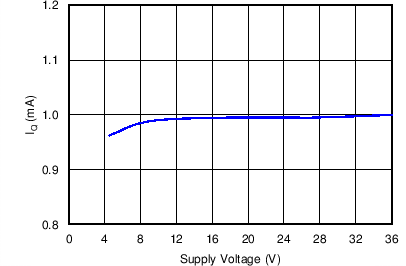
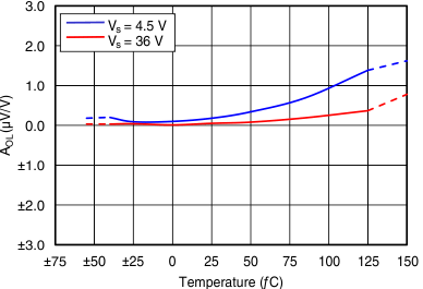
| RL = 10 kΩ | ||
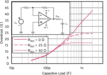
| RI = 1 kΩ | RF = 1 kΩ | G = –1 |
(100-mV Output Step)
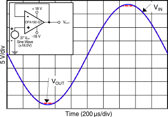
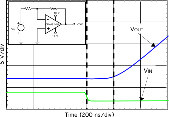
| RI = 1 kΩ | G = –10 | RF = 10 kΩ |
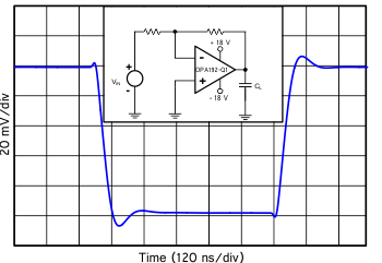
| RL = 1 kΩ | CL = 10 pF | G = –1 |
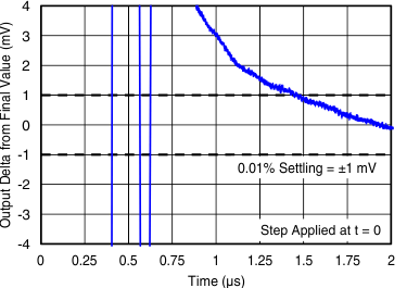
| G = 1 | ||
| G = 1 | ||
