ZHCSGC1F June 2017 – March 2021 OPA145 , OPA2145
PRODUCTION DATA
- 1 特性
- 2 应用
- 3 说明
- 4 Revision History
- 5 Pin Configuration and Functions
- 6 Specifications
- 7 Detailed Description
- 8 Application and Implementation
- 9 Power Supply Recommendations
- 10Layout
- 11Device and Documentation Support
- 12Mechanical, Packaging, and Orderable Information
封装选项
机械数据 (封装 | 引脚)
散热焊盘机械数据 (封装 | 引脚)
- DGK|8
订购信息
8.3.1 16-Bit, 100-kSPS, Fully Differential Transimpedance Imaging and Measurement
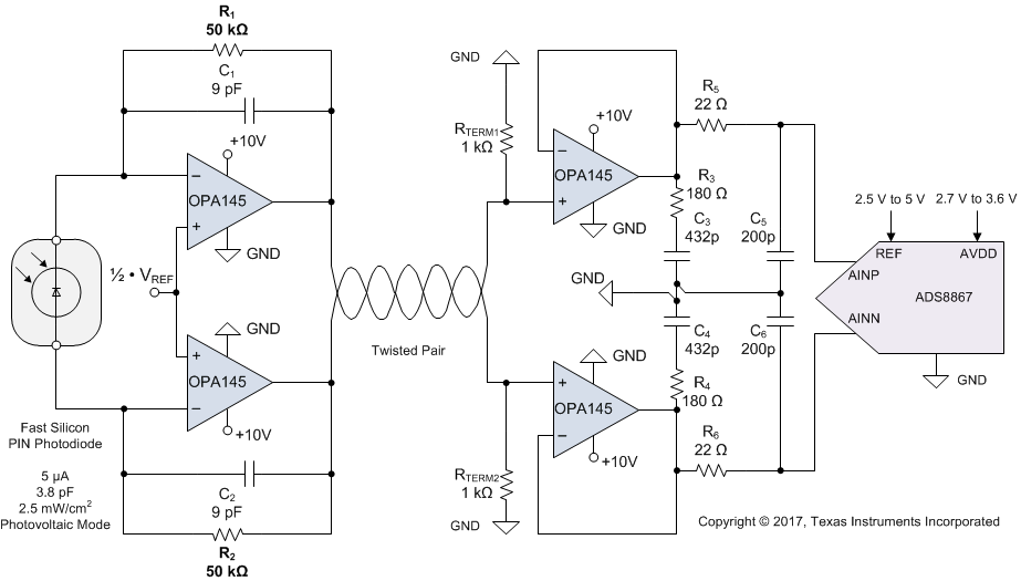
The OPAx145 are used in a differential transimpedance (I-V) measurement application capable of driving the ADS8867, a 16-bit, microPower, truly-differential ADC, at its maximum conversion rate of 100 kSPS with an acquisition time of 1200 ns and conversion time of 8800 ns. The first stage supports a forward bandwidth of 493.5 kHz with 100 kΩ of transimpedance gain, enabling the photodiode to fully charge and settle to ±38 µV (±1/2 LSB on 5-V ADC reference voltage) within the conversion time of the ADC. The differential nature of the system provides several advantages such as double the transimpedance gain compared to a single-ended system, improved signal-to-noise ratio, easy interfacing to high-precision, fully-differential ADCs, and additional protection against inductively-coupled noise and interference. Additionally, capacitively-coupled common-mode transients can be minimized using low-impedance termination resistors RTERM1 and RTERM2.
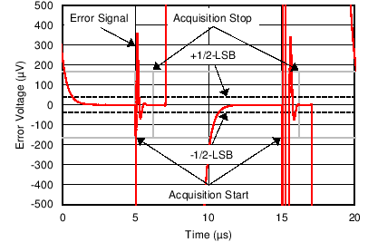
The second stage provides the reverse bandwidth required for settling to 16-bit accuracy after the internal sampling capacitor of the successive-approximation-register (SAR) ADC is connected to the second stage. The two OPAx145 amplifiers in the second stage are configured as buffers for maximum closed-loop bandwidth, and their stability is optimized using R3, C3 and R4, C4 by creating a snubber that reduces the open-loop output impedance (see Figure 6-26). C5 and C6 are provided as a charge reservoir for the internal sampling capacitor of the ADC, and R5 and R6 are tuned to optimize the phase margin of the second stage to drive the output capacitance. This two-stage approach enables compatibility with a wide selection of high output-impedance sensors while still maintaining 16-bit settling performance. Furthermore, the first stage can be designed with sufficient phase margin to drive twisted-pair transmission lines in remote measurement systems. Proper design of the transmission line reduces the interference of other signals over long distances. Figure 8-4 shows the settling performance of the system described previously and in Figure 8-3 — the settling time during the acquisition cycle is shown for settling successfully to 0 µA from 5 µs to 6.2 µs. At 6.3 µs, the photodiode current is changed to 5 µA (full-scale) and settles during the conversion cycle of the ADC (6.2 µs to 15 µs), and is then acquired successfully from 15 µs to 16.2 µs.
 Figure 8-3 16-bit, 100-kSPS, Fully Differential Transimpedance Schematic
 Figure 8-4 16-bit, 100-kSPS, Fully Differential Transimpedance Settling Performance