ZHCSGK6 July 2017 ONET2804TLP
PRODUCTION DATA.
- 1 特性
- 2 应用
- 3 说明
- 4 修订历史记录
- 5 Pin Configuration and Functions
- 6 Specifications
-
7 Detailed Description
- 7.1 Overview
- 7.2 Functional Block Diagram
- 7.3 Feature Description
- 7.4 Device Functional Modes
- 7.5 Programming
- 7.6
Register Maps
- 7.6.1 Register Descriptions
- 7.6.2 Register 0: Control Settings (address = 00h) [reset = 0h]
- 7.6.3 Register 1: Amplitude and Rate for Channel 1 (address = 01h) [reset = 0h]
- 7.6.4 Register 2: Threshold and Gain for Channel 1 (address = 02h) [reset = 0h]
- 7.6.5 Register 7: Amplitude and Rate for Channel 2 (address = 07h) [reset = 0h]
- 7.6.6 Register 8: Threshold and Gain for Channel 1 (address = 08h) [reset = 0h]
- 7.6.7 Register 13: Amplitude and Rate for Channel 3 (address = 0Dh) [reset = 0h]
- 7.6.8 Register 14: Threshold and Gain for Channel 3 (address = 0Eh) [reset = 0h]
- 7.6.9 Register 19: Amplitude and Rate for Channel 4 (address = 13h) [reset = 0h]
- 7.6.10 Register 20: Threshold and Gain for Channel 4 (address = 14h) [reset = 0h]
- 8 Application and Implementation
- 9 Power Supply Recommendations
- 10Layout
- 11器件和文档支持
- 12机械、封装和可订购信息
8 Application and Implementation
NOTE
Information in the following applications sections is not part of the TI component specification, and TI does not warrant its accuracy or completeness. TI’s customers are responsible for determining suitability of components for their purposes. Customers should validate and test their design implementation to confirm system functionality.
8.1 Application Information
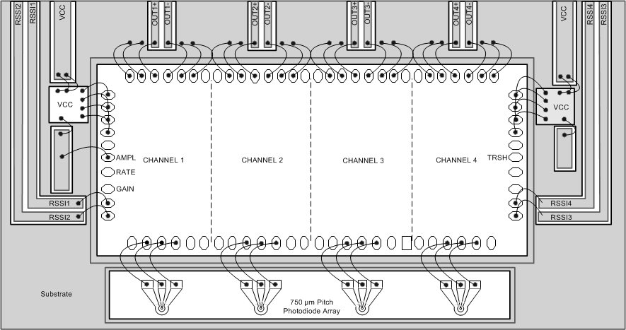
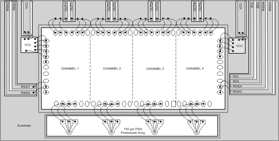
Figure 24 shows the ONET2804TLP being used in a fiber optic receiver application with four channels running at 25 Gbps each and with pin control. Figure 27 illustrates the device being used with two-wire control. The ONET2804TLP converts the electrical current generated by the PIN photodiode into a differential output voltage. The FILTERx inputs provide a DC bias voltage for the PIN that is low-pass filtered. The photodiode must be connected to the FILTERx pads for the bias circuit to function correctly because the voltage drop across the photodiode FET is sensed and used by the bias circuit.
The RSSIx outputs are used to mirror the photodiode output current and can be connected via resistors to GND. The voltage gain can be adjusted for the intended application by choosing the external resistor; however, for proper operation of the ONET2804TLP, ensure that the voltage at RSSIx never exceeds VCC – 0.65 V. If the RSSIx outputs are not used when using the internal PD bias, then leave these outputs open.
The OUTx+ and OUTx– pins are internally terminated by 50-Ω pullup resisters to VCC. The outputs must be AC coupled (for example, by using 0.1-µF capacitors) to the succeeding device.
8.2 Typical Applications
8.2.1 Pad Control Application
 Figure 24. Basic Application Circuit with Pad Control
8.2.1.1 Design Requirements
Table 13. Design Parameters
| PARAMETER | VALUE |
|---|---|
| Input voltage | 3.3 V |
| Output voltage | 300 mVPP |
8.2.1.2 Detailed Design Procedure
The ONET2804TLP is designed to be used in conjunction with a 750-μm pitch photodiode array or individual photodiodes and assembled into a receiver optical subassembly (ROSA). The TIA is typically mounted on a ceramic substrate with etched connections for VCC, RSSIx, and 100-Ω differential transmission lines for the output voltage. The photodiode converts the optical input signal into a current that is supplied to the TIA through wire bonds. The TIA then converts the input current into a voltage and further amplifies the signal. TI recommends setting the output amplitude to the 300-mVPP level by leaving AMPL (pad 6) floating.
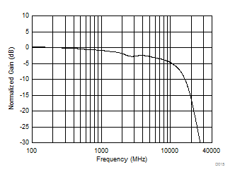
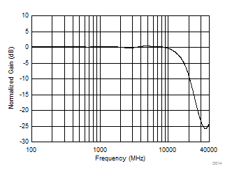
The ROSA is typically mounted on a printed circuit board (PCB) with 100-Ω differential transmission lines and RF connectors [such as GPPO® or 2.4-mm subminiature version A (SMA) connectors]. When measuring the output from the ROSA mounted on the PCB, the frequency dependent loss of the transmission lines affects the frequency response. The loss can be de-embedded from the measurement to determine the actual frequency response at the output of the ROSA.
8.2.1.3 Application Curves


8.2.2 Two-Wire Control Application
 Figure 27. Basic Application Circuit with Two-Wire Control
8.2.2.1 Design Requirements
Table 14 lists the design requirements for this application.
Table 14. Design Parameters
| PARAMETER | VALUE |
|---|---|
| I2CENA pin voltage | 3.3 V |
| Output voltage | 300 mVPP |
8.2.2.2 Detailed Design Procedure
As described in the Detailed Design Procedure section on the pad control application, TI generally recommends setting the output voltage of the device to the 300-mVPP setting. The output voltage setting can be controlled by bonding specific device pads as detailed in the Pad Control Application section, but can alternatively be controlled using the device I2C interface. To set the output amplitude via the I2C interface, the I2CENA pad must be connected to VCC, which enables the I2C control and disables pad control. The output amplitude can then be set to the 300-mVPP mode by writing the value 0110 to bits[3:0] of the amplitude control registers for each channel as described in the Register Maps section. Requirements to operate the I2C interface are detailed in the Programming section.