SLVS033G February 1990 – July 2015 LT1054
PRODUCTION DATA.
- 1 Features
- 2 Applications
- 3 Description
- 4 Revision History
- 5 Pin Configuration and Functions
- 6 Specifications
- 7 Detailed Description
- 8 Application and Implementation
- 9 Power Supply Recommendations
- 10Layout
- 11Device and Documentation Support
- 12Mechanical, Packaging, and Orderable Information
封装选项
请参考 PDF 数据表获取器件具体的封装图。
机械数据 (封装 | 引脚)
- P|8
- DW|16
散热焊盘机械数据 (封装 | 引脚)
- DW|16
订购信息
7 Detailed Description
7.1 Overview
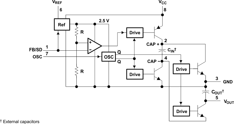
LT1054 is a "negative voltage generator" or "negative charge pump" that will output a negative voltage that is proportional to the input voltage (or VCC). With proper supply voltage, VOUT will regulate to an unregulated VOUT that is approximately –VCC (reduced by a small voltage loss). If a lower absolute voltage is desired, VOUT can be regulated to that value when proper feedback resistors are applied.
LT1054 regulates up to 100mA with minimal loss and has a shutdown mode that makes this part optimal across a wide range of applications.
7.2 Functional Block Diagram
7.3 Feature Description
7.3.1 Reference and Error Amplifier for Regulation
The feedback/shutdown (FB/SD) terminal has two functions. Pulling FB/SD below the shutdown threshold (≈ 0.45 V) puts the device into shutdown. In shutdown, the reference/regulator is turned off and switching stops. The switches are set such that both CIN and COUT are discharged through the output load. Quiescent current in shutdown drops to approximately 100 µA. Any open-collector gate can be used to put the LT1054 into shutdown. For normal (unregulated) operation, the device will restart when the external gate is shut off. In LT1054 circuits that use the regulation feature, the external resistor divider can provide enough pulldown to keep the device in shutdown until the output capacitor (COUT) has fully discharged. For most applications, where the LT1054 is run intermittently, this does not present a problem because the discharge time of the output capacitor is short compared to the off time of the device. In applications where the device has to start up before the output capacitor (COUT) has fully discharged, a restart pulse must be applied to FB/SD of the LT1054. Using the circuit shown in Figure 11, the restart signal can be either a pulse (tp > 100 µs) or a logic high. Diode coupling the restart signal into FB/SD allows the output voltage to rise and regulate without overshoot. The resistor divider R3/R4 shown in Figure 11 should be chosen to provide a signal level at FB/SD of 0.7−1.1 V.
FB/SD also is the inverting input of the LT1054 error amplifier and, as such, can be used to obtain a regulated output voltage.
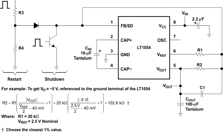 Figure 11. Basic Regulation Configuration
7.3.2 External Oscillator Synchronization
This pin can be used to raise or lower the oscillator frequency or to synchronize the device to an external clock. Internally Pin 7 is connected to the oscillator timing capacitor (Ct ≈ 150pF) which is alternately charged and discharged by current sources of ±7µA so that the duty cycle is ≈50%. The LT1054 oscillator is designed to run in the frequency band where switching losses are minimized. However the frequency can be raised, lowered, or synchronized to an external system clock if necessary.
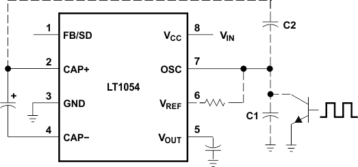 Figure 12. External-Clock System
The frequency can be lowered by adding an external capacitor (C1, Figure 12) from Pin 7 to ground. This will increase the charge and discharge times which lowers the oscillator frequency. The frequency can be increased by adding an external capacitor (C2, Figure 12, in the range of 5pF to 20pF) from Pin 2 to Pin 7. This capacitor will couple charge into CT at the switch transitions, which will shorten the charge and discharge time, raising the oscillator frequency. Synchronization can be accomplished by adding an external resistive pull-up from Pin 7 to the reference pin (Pin 6). A 20k pull-up is recommended. An open collector gate or an NPN transistor can then be used to drive the oscillator pin at the external clock frequency as shown in Figure 12. Pulling up Pin 7 to an external voltage is not recommended. For circuits that require both frequency synchronization and regulation, an external reference can be used as the reference point for the top of the R1/R2 divider allowing Pin 6 to be used as a pullup point for Pin 7.
7.3.3 Output Current and Voltage Loss
The functional block diagram shows that the maximum regulated output voltage is limited by the supply voltage. For the basic configuration, |VOUT| referenced to the ground terminal of the LT1054 must be less than the total of the supply voltage minus the voltage loss due to the switches. The voltage loss versus output current due to the switches can be found in the typical performance curves. Other configurations, such as the negative doubler, can provide higher voltages at reduced output currents.
7.3.4 Reference Voltage
Reference Output. This pin provides a 2.5V reference point for use in LT1054-based regulator circuits. The temperature coefficient of the reference voltage has been adjusted so that the temperature coefficient of the regulated output voltage is close to zero. This requires the reference output to have a positive temperature coefficient as can be seen in the typical performance curves. This nonzero drift is necessary to offset a drift term inherent in the internal reference divider and comparator network tied to the feedback pin. The overall result of these drift terms is a regulated output which has a slight positive temperature coefficient at output voltages below 5V and a slight negative TC at output voltages above 5V. Reference output current should be limited, for regulator feedback networks, to approximately 60µA. The reference pin will draw ≈100µA when shorted to ground and will not affect the internal reference/regulator, so that this pin can also be used as a pull-up for LT1054 circuits that require synchronization.
7.4 Device Functional Modes
7.4.1 Main Operation
A review of a basic switched-capacitor building block is helpful in understanding the operation of the LT1054. When the switch shown in Figure 13 is in the left position, capacitor C1 charges to the voltage at V1. The total charge on C1 is q1 = C1*V1. When the switch is moved to the right, C1 is discharged to the voltage at V2. After this discharge time, the charge on C1 is q2 = C1*V2. The charge has been transferred from the source V1 to the output V2. The amount of charge transferred is shown in Equation 1.
If the switch is cycled f times per second, the charge transfer per unit time (that is, current) is as shown in Equation 2.
To obtain an equivalent resistance for a switched-capacitor network, this equation can be rewritten in terms of voltage and impedance equivalence as shown in Equation 3.

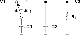 Figure 13. Switched-Capacitor Building Block
A new variable, REQUIV, is defined as REQUIV = 1 / (f × C1). The equivalent circuit for the switched-capacitor network is shown in Figure 14. The LT1054 has the same switching action as the basic switched-capacitor building block. Even though this simplification does not include finite switch-on resistance and output-voltage ripple, it provides an insight into how the device operates.
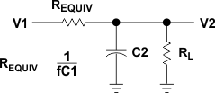 Figure 14. Switched-Capacitor Equivalent Circuit
These simplified circuits explain voltage loss as a function of oscillator frequency (see Figure 7). As oscillator frequency is decreased, the output impedance eventually is dominated by the 1 / (f × C1) term, and voltage losses rise.
Voltage losses also rise as oscillator frequency increases. This is caused by internal switching losses that occur due to some finite charge being lost on each switching cycle. This charge loss per-unit-cycle, when multiplied by the switching frequency, becomes a current loss. At high frequency, this loss becomes significant and voltage losses again rise.
The oscillator of the LT1054 is designed to operate in the frequency band where voltage losses are at a minimum.
7.4.2 Shutdown
LT1054 can be put into a low quiescent current state by grounding the FB/SD pin. Once FB/SD is pulled low, current being drawn from the supply will be approximately 100 µA.