SNOSAG7D August 2005 – August 2016 LPV511
PRODUCTION DATA.
8 Application and Implementation
NOTE
Information in the following applications sections is not part of the TI component specification, and TI does not warrant its accuracy or completeness. TI’s customers are responsible for determining suitability of components for their purposes. Customers should validate and test their design implementation to confirm system functionality.
8.1 Application Information
The LPV511 is fabricated with Texas Instrument's state-of-the-art VIP50C process.
8.2 Typical Applications
8.2.1 Battery Current Sensing
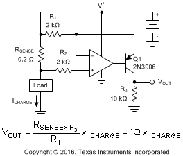
The rail-to-rail common mode input range and the very low quiescent current make the LPV511 ideal to use in high-side and low-side battery current sensing applications. The high-side current sensing circuit in Figure 28 is commonly used in a battery charger to monitor the charging current to prevent over charging. A sense resistor RSENSE is connected to the battery directly.
 Figure 28. High Side Current Sensing
8.2.1.1 Design Requirements
The high-side current-sensing circuit (Figure 28) is commonly used in a battery charger to monitor charging current to prevent overcharging. A sense resistor RSENSE is connected to the battery directly. This system requires an op amp with rail-to-rail input. The LPV511 ideal for this application because its common-mode input range extends up to the positive supply.
8.2.1.2 Detailed Design Procedure
As seen in Figure 28, the ICHARGE current flowing through sense resistor RSENSE develops a voltage drop equal to VSENSE. The voltage at the negative sense point will now be less than the positive sense point by an amount proportional to the VSENSE voltage.
The low-bias currents of the LPV511 cause little voltage drop through R2, so the negative input of the LPV551 amplifier is at essentially the same potential as the negative sense input.
The LPV511 will detect this voltage error between its inputs and servo the transistor base to conduct more current through Q1, increasing the voltage drop across R1 until the LPV511 inverting input matches the noninverting input. At this point, the voltage drop across R1 now matches VSENSE.
IG, a current proportional to ICHARGE, will flow according to the following relation to:
IG also flows through the gain resistor R3 developing a voltage drop equal to:
where
- G = R3 / R1
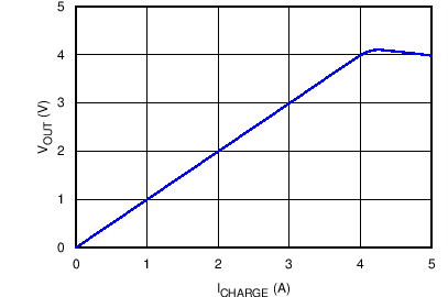
8.2.1.3 Application Curve
Figure 29 shows the results of the example current sense circuit.

8.2.2 Summing Amplifier
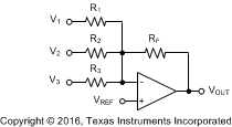
The LPV511 operational amplifier is a perfect fit in a summing amplifier circuit because of the rail-to-rail input and output and the sub-micro Amp quiescent current. In this configuration, the amplifier outputs the sum of the three input voltages.
Equation 4 shows the ratio of the sum and the output voltage is defined using feedback and input resistors.

 Figure 30. Summing Amplifier Circuit
8.3 Dos and Don'ts
Do properly bypass the power supplies.
Do add series resistence to the output when driving capacitive loads, particularly cables, Muxes and ADC inputs.
Do add series current limiting resistors and external Schottky clamp diodes if input voltage is expected to exceed the supplies. Limit the current to 1 mA or less (1 kΩ per volt).