SNVS458D June 2007 – October 2016 LP55281
PRODUCTION DATA.
- 1 Features
- 2 Applications
- 3 Description
- 4 Revision History
- 5 Pin Configuration and Functions
- 6 Specifications
- 7 Detailed Description
- 8 Application and Implementation
- 9 Power Supply Recommendations
- 10Layout
- 11Device and Documentation Support
- 12Mechanical, Packaging, and Orderable Information
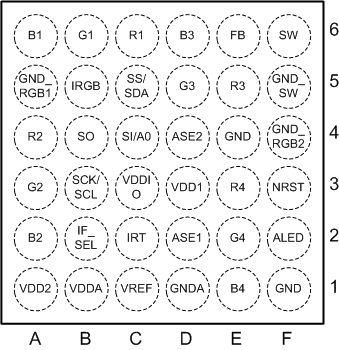
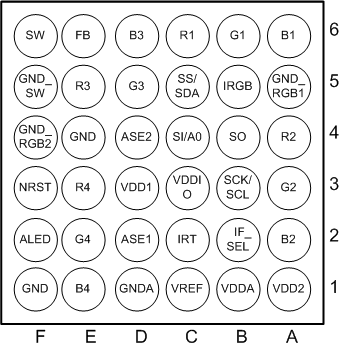
5 Pin Configuration and Functions
YPG and YZR Packages
36-Pin DSBGA
Top View

YPG and YZR Packages
36-Pin DSBGA
Bottom View

Pin Functions
| PIN | TYPE | DESCRIPTION | |
|---|---|---|---|
| NUMBER | NAME | ||
| 1A | VDD2 | Power | Supply voltage |
| 1B | VDDA | Power | Internal LDO output |
| 1C | VREF | Output | Reference voltage |
| 1D | GNDA | Ground | Ground for analog circuitry |
| 1E | B4 | Output | Blue LED 4 output |
| 1F | GND | Ground | Ground |
| 2A | B2 | Output | Blue LED 2 output |
| 2B | IF_SEL | Logic Input | Interface (SPI or I2C compatible) selection (IF_SEL = 1 for SPI) |
| 2C | IRT | Input | Oscillator frequency resistor |
| 2D | ASE1 | Input | Audio synchronization input 1 |
| 2E | G4 | Output | Green LED 4 output |
| 2F | ALED | Output | Audio Synchronized LED oautput |
| 3A | G2 | Output | Green LED 2 output |
| 3B | SCK/SCL | Logic Input | Clock (SPI/I2C) |
| 3C | VDDIO | Power | Supply voltage for input/output buffers and drivers |
| 3D | VDD1 | Power | Supply voltage |
| 3E | R4 | Output | Red LED 4 output |
| 3F | NRST | Input | Asynchronous reset, active low |
| 4A | R2 | Output | Red LED 2 output |
| 4B | SO | Logic Output | Serial data out (SPI) |
| 4C | SI/A0 | Logic Input | Serial input (SPI), address select (I2C) |
| 4D | ASE2 | Input | Audio synchronization input 2 |
| 4E | GND | Ground | Ground |
| 4F | GND_RGB2 | Ground | Ground for RGB3-4 currents |
| 5A | GND_RGB1 | Ground | Ground for RGB1-2 currents |
| 5B | IRGB | Input | Bias current set resistor for RGB drivers |
| 5C | SS/SDA | Logic Input/Output | Slave select (SPI), Serial data in/out (I2C) |
| 5D | G3 | Output | Green LED 3 output |
| 5E | R3 | Output | Red LED 3 output |
| 5F | GND_SW | Ground | Power switch ground |
| 6A | B1 | Output | Blue LED 1 output |
| 6B | G1 | Output | Green LED 1 output |
| 6C | R1 | Output | Red LED 1 output |
| 6D | B3 | Output | Blue LED 3 output |
| 6E | FB | Input | Boost converter feedback |
| 6F | SW | Output | Boost converter power switch |