SNVS482F January 2007 – December 2015
PRODUCTION DATA.
- 1 Features
- 2 Applications
- 3 Description
- 4 Revision History
- 5 Pin Configuration and Functions
- 6 Specifications
- 7 Detailed Description
- 8 Application and Implementation
- 9 Power Supply Recommendations
- 10Layout
- 11Device and Documentation Support
- 12Mechanical, Packaging, and Orderable Information
封装选项
机械数据 (封装 | 引脚)
散热焊盘机械数据 (封装 | 引脚)
订购信息
7 Detailed Description
7.1 Overview
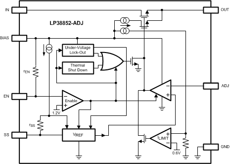
The LP38852-ADJ is a high-current, low-dropout, fast-response linear regulator capable of sourcing 1.5-A load with only 130-mV dropout. This device operates from two input voltages: VBIAS provides voltage to internal circuit, while VIN is the input voltage supplying power to load. The use of an external bias rail allows the part to operate from ultra-low VIN voltages. The fast transient response of this device makes it suitable for powering DSP, microcontroller cores, and post-regulators.
7.2 Functional Block Diagram

7.3 Feature Description
7.3.1 Undervoltage Lockout (UVLO)
The bias voltage is monitored by a circuit which prevents the device from functioning when the bias voltage is below the UVLO threshold of approximately 2.45 V.
As the bias voltage rises above the UVLO threshold the device control circuitry becomes active. There is approximately 150 mV of hysteresis built into the UVLO threshold to provide noise immunity.
When the bias voltage is between the UVLO threshold and the minimum operating rating value of 3 V the device is functional, but the operating parameters are not within the specified limits.
7.3.2 Supply Sequencing
There is no requirement for the order that VIN or VBIAS are applied or removed.
One practical limitation is that the soft-start circuit starts charging soft-start timing capacitor (CSS) when both VBIAS rises above the UVLO threshold and the EN pin is above the VEN(ON) threshold. If the application of VIN is delayed beyond this point the benefits of soft start is compromised.
In any case, the output voltage cannot be ensured until both VIN and VBIAS are within the range of specified operating values.
If used in a dual-supply system where the regulator output load is returned to a negative supply, the OUT pin must be diode clamped to ground. A Schottky diode is recommended for this diode clamp.
7.3.3 Reverse Voltage
A reverse voltage condition exists when the voltage at the OUT pin is higher than the voltage at the IN pin. Typically this happens when VIN is abruptly taken low, and COUT continues to hold a sufficient charge such that the input to output voltage becomes reversed.
The NMOS pass element, by design, contains no body diode. This means that, as long as the gate of the pass element is not driven, there is no reverse current flow through the pass element during a reverse voltage event. The gate of the pass element is not driven when VBIAS is below the UVLO threshold, or when the EN pin is held low.
When VBIAS is above the UVLO threshold, and the EN pin is above the VEN(ON) threshold, the control circuitry is active and attempts to regulate the output voltage. Because the input voltage is less than the output voltage the control circuit drives the gate of the pass element to the full VBIAS potential when the output voltage begins to fall. In this condition, reverse current flows from the OUT pin to the IN pin , limited only by the RDS(ON) of the pass element and the output-to-input voltage differential. Discharging an output capacitor up 1000 µF in this manner does not damage the device as the current rapidly decays. However, continuous reverse current must be avoided.
7.3.4 Soft-Start
The LP38852-ADJ incorporates a soft-start function that reduces the start-up current surge into the output capacitor (COUT) by allowing VOUT to rise slowly to the final value. This is accomplished by controlling VREF at the SS pin. CSS is internally held to ground until both VBIAS rises above the UVLO threshold and the EN pin is higher than the VEN(ON) threshold.
VREF rises at an RC rate defined by the internal resistance of the SS pin (rSS) and the external capacitor connected to the SS pin. This allows the output voltage to rise in a controlled manner until steady-state regulation is achieved. Typically, five time constants are recommended to assure that the output voltage is sufficiently close to the final steady-state value. During the soft-start time the output current can rise to the built-in current limit.
Because the VOUT rise is exponential, not linear, the in-rush current peaks during the first time constant (τ), and VOUT requires four additional time constants (4τ) to reach the final value (5τ) .
After achieving normal operation, if either VBIAS falls below the ULVO threshold, or the EN pin falls below the VEN(OFF) threshold, the device output is disabled, and the CSS discharge circuit becomes active. The CSS discharge circuit remains active until VBIAS falls to 500 mV (typical). When VBIAS falls below 500 mV (typical), the CSS discharge circuit ceases to function due to a lack of sufficient biasing to the control circuitry.
Because VREF appears on the SS pin, any leakage through CSS causes VREF to fall, thus affecting VOUT. A leakage of 50 nA (about 10 MΩ) through CSS causes VOUT to be approximately 0.1% lower than nominal, while a leakage of 500 nA (about 1 MΩ) causes VOUT to be approximately 1% lower than nominal. Typical ceramic capacitors have a factor of 10× difference in leakage between 25°C and 85°C, so the maximum ambient temperature must be included in the capacitor selection process.
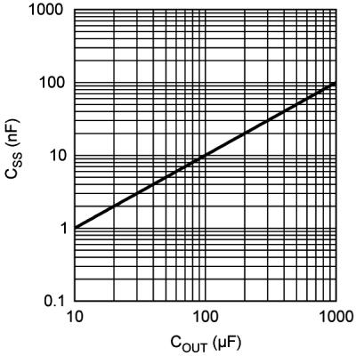
Typical CSS values are in the range of 1 nF to 100 nF, providing typical soft-start times in the range of 70 μs to 7 ms (5τ). Values less than 1 nF may be used, but the soft-start effect is minimal. Values larger than 100 nF provide soft start but may not be fully discharged if VBIAS falls from the UVLVO threshold to less than 500 mV in less than 100 µs.
Figure 22 shows the relationship between the COUT value and a typical CSS value.
 Figure 22. Typical CSS vs COUT Values
The CSS capacitor must be connected to a clean ground path back to the device ground pin. No components, other than CSS, should be connected to the SS pin, as there could be adverse effects to VOUT.
If the soft-start function is not needed the SS pin must be left open, although some minimal capacitance value is always recommended.
7.3.5 Setting The Output Voltage
The output voltage is set using the external resistive divider R1 and R2. (Refer to the Figure 23.) The output voltage is given by Equation 2:

The resistors used for R1 and R2 must be high quality, tight tolerance, and with matching temperature coefficients. It is important to remember that, although the value of VADJ is specified, the use of low quality resistors for R1 and R2 can easily produce a VOUT value that is unacceptable.
It is recommended that the values selected for R1 and R2 are such that the parallel value is less than 10 kΩ. This is to prevent internal parasitic capacitances on the ADJ pin from interfering with the FZ pole set by R1 and CFF.
Table 1 lists some suggested, best fit, standard ±1% resistor values for R1 and R2, and a standard ±10% capacitor values for CFF, for a range of VOUT values. Other values of R1, R2, and CFF are available that give similar results.
Table 1. Suggested Resistor Values
| VOUT | R1 | R2 | CFF | FZ |
|---|---|---|---|---|
| 0.8 V | 1.07 kΩ | 1.78 kΩ | 12 nF | 12.4 kHz |
| 0.9 V | 1.50 kΩ | 1.87 kΩ | 8.2 nF | 12.9 kHz |
| 1 V | 1.00 kΩ | 1.00 kΩ | 12 nF | 13.3 kHz |
| 1.1 V | 1.65 kΩ | 1.37 kΩ | 8.2 nF | 11.8 kHz |
| 1.2 V | 1.40 kΩ | 1.00 kΩ | 10 nF | 11.4 kHz |
| 1.3 V | 1.15 kΩ | 715 Ω | 12 nF | 11.5 kHz |
| 1.4 V | 1.07 kΩ | 590 Ω | 12 nF | 12.4 kHz |
| 1.5 V | 2.00 kΩ | 1.00 kΩ | 6.8 nF | 11.7 kHz |
| 1.6 V | 1.65 kΩ | 750 Ω | 8.2 nF | 11.8 kHz |
| 1.7 V | 2.55 kΩ | 1.07 kΩ | 5.6 nF | 11.1 kHz |
| 1.8 V | 2.94 kΩ | 1.13 kΩ | 4.7 nF | 11.5 kHz |
Please refer to the TI Application Note AN-1378 Method for Calculating Output Voltage Tolerances in Adjustable Regulators (SNVA112) for additional information on how resistor tolerances affect the calculated VOUT value.
7.3.6 Enable (EN)
The EN pin provides a mechanism to enable, or disable, the regulator output stage. The EN pin has an internal pullup to VBIAS through a 180-kΩ (typical) resistor. The EN pin can be left open or connected VBIAS if the enable function is not needed.
7.4 Device Functional Modes
7.4.1 Input Voltage
The input voltage (VIN) is the high-current external voltage rail that is regulated down to a lower voltage, which is applied to the load. The input voltage must be at least VOUT + VDO and no higher than whatever value is used for VBIAS.
For applications where VBIAS is higher than 4.5 V, VIN must be no greater than 4.5 V, otherwise output voltage accuracy may be affected.
7.4.2 Bias Voltage
The bias voltage (VBIAS) is a low-current external voltage rail required to bias the control circuitry and provide gate drive for the N-FET pass transistor. When VOUT is set to 1.2 V, or less, VBIAS may be anywhere in the operating range of 3 V to 5.5 V. If VOUT is set higher than 1.2 V , VBIAS must be between 4.5 V and 5.5 V to ensure proper operation of the device.
7.4.3 Enable (EN) Operation
If the EN pin is actively driven, pulling the EN pin above the VEN threshold of 1.25 V (typical) turns on the regulator output; pulling the EN pin below the VEN threshold turns off the regulator output. There is approximately 100 mV of hysteresis built into the enable threshold provide noise immunity.
If the enable function is not needed the EN pin must be left open, or connected directly to VBIAS. If the EN pin is left open, stray capacitance on this pin must be minimized; otherwise, the output turnon is delayed while the stray capacitance is charged through the internal resistance (rEN).