ZHCSAZ8K January 2005 – January 2016 LP38691-ADJ , LP38691-ADJ-Q1 , LP38693-ADJ , LP38693-ADJ-Q1
PRODUCTION DATA.
- 1 特性
- 2 应用范围
- 3 说明
- 4 修订历史记录
- 5 Pin Configuration and Functions
- 6 Specifications
- 7 Detailed Description
-
8 Application and Implementation
- 8.1 Application Information
- 8.2
Typical Applications
- 8.2.1 Design Requirements
- 8.2.2 Detailed Design Procedure
- 8.2.3 Application Curve
- 9 Power Supply Recommendations
- 10Layout
- 11器件和文档支持
- 12机械、封装和可订购信息
10 Layout
10.1 Layout Guidelines
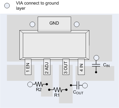
Good PC layout practices must be used or instability can be induced because of ground loops and voltage drops. The input and output capacitors must be directly connected to the input, output, and ground pins of the regulator using traces which do not have other currents flowing in them (Kelvin connect).
The best way to do this is to lay out CIN and COUT near the device with short traces to the IN, OUT, and GND pins. The regulator ground pin should be connected to the external circuit ground so that the regulator and its capacitors have a "single point ground."
It should be noted that stability problems have been seen in applications where "vias" to an internal ground plane were used at the ground points of the device and the input and output capacitors. This was caused by varying ground potentials at these nodes resulting from current flowing through the ground plane. Using a single point ground technique for the regulator and its capacitors fixed the problem. Because high current flows through the traces going into VIN and coming from VOUT, Kelvin connect the capacitor leads to these pins so there is no voltage drop in series with the input and output capacitors.
10.2 Layout Examples

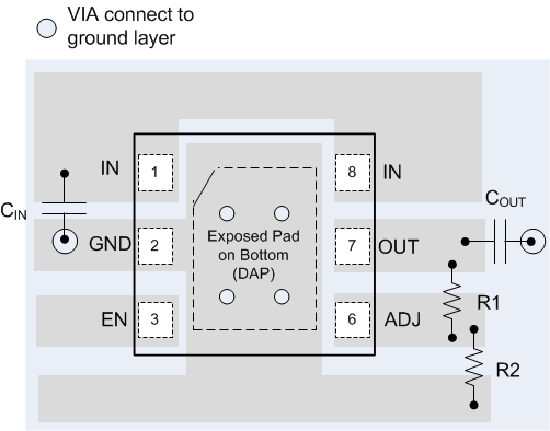
 Figure 32. WSON LP38693 Layout
10.3 WSON Mounting
The NGG0006A (No Pullback) 6-Lead WSON package requires specific mounting techniques which are detailed in the TI Application ReportLeadless Leadframe Package (LLP) SNOA401. Referring to the section PCB Design Recommendations, it should be noted that the pad style which should be used with the WSON package is the NSMD (non-solder mask defined) type. Additionally, it is recommended the PCB terminal pads to be 0.2 mm longer than the package pads to create a solder fillet to improve reliability and inspection.
The thermal dissipation of the WSON package is directly related to the printed circuit board construction and the amount of additional copper area connected to the DAP. The DAP (exposed pad) on the bottom of the WSON package is connected to the die substrate with a conductive die attach adhesive. The DAP has no direct electrical (wire) connection to any of the pins. There is a parasitic PN junction between the die substrate and the device ground. As such, it is strongly recommend that the DAP be connected directly to the ground at device pin 2 (GND). Alternatively, but not recommended, the DAP may be left floating (no electrical connection). The DAP must not be connected to any potential other than ground.