ZHCSAS0L January 2005 – December 2014 LP38691 , LP38691-Q1 , LP38693 , LP38693-Q1
PRODUCTION DATA.
- 1 特性
- 2 应用范围
- 3 说明
- 4 典型应用电路
- 5 修订历史记录
- 6 Pin Configuration and Functions
- 7 Specifications
- 8 Detailed Description
- 9 Application and Implementation
- 10Power Supply Recommendations
- 11Layout
- 12器件和文档支持
- 13机械封装和可订购信息
8 Detailed Description
8.1 Overview
The LP38691/93 are designed to meet the requirements of portable, battery-powered digital systems providing an accurate output voltage with fast start-up. When disabled via a low logic signal at the enable pin (EN), the power consumption is reduced to virtually zero (LP38693 only).
The LP38691/93 will perform well with a single 1-μF input capacitor and a single 1-μF ceramic output capacitor.
8.2 Functional Block Diagrams
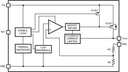 Figure 23. LP38691 Functional Diagram (WSON)
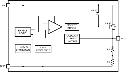 Figure 24. LP38691 Functional Diagram (TO-252)
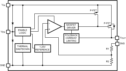 Figure 25. LP38693 Functional Diagram (WSON)
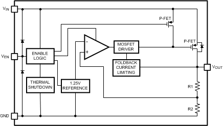 Figure 26. LP38693 Functional Diagram (SOT-223)
8.3 Feature Description
8.3.1 Enable (EN)
The LP38693 has an Enable pin (EN) which allows an external control signal to turn the regulator output On and Off. The Enable On/Off threshold has no hysteresis. The voltage signal must rise and fall cleanly, and promptly, through the ON and OFF voltage thresholds. The EN pin voltage must be higher than the VEN(MIN) threshold to ensure that the device is fully enabled under all operating conditions. The EN pin voltage must be lower than the VEN(MAX) threshold to ensure that the device is fully disabled. The EN pin has no internal pullup or pulldown to establish a default condition and, as a result, this pin must be terminated either actively or passively. If the EN pin is driven from a source that actively pulls high and low, the drive voltage should not be allowed to go below ground potential or higher than VIN. If the application does not require the Enable function, the pin should be connected directly to the VIN pin.
8.3.2 Thermal Overload Protection (TSD)
Thermal Shutdown disables the output when the junction temperature rises to approximately 160°C which allows the device to cool. When the junction temperature cools to approximately 150°C, the output circuitry enables.
Based on power dissipation, thermal resistance, and ambient temperature, the thermal protection circuit may cycle on and off. This thermal cycling limits the dissipation of the regulator and protects it from damage as a result of overheating. The Thermal Shutdown circuitry of the LP38693 has been designed to protect against temporary thermal overload conditions.
The Thermal Shutdown circuitry was not intended to replace proper heat-sinking. Continuously running the LP38693 device into thermal shutdown degrades device reliability.
8.3.3 Foldback Current Limiting
Foldback current limiting is built into the LP38691 and LP38693 devices which reduces the amount of output current the part can deliver as the output voltage is reduced. The amount of load current is dependent on the differential voltage between VIN and VOUT. Typically, when this differential voltage exceeds 5 V, the load current will limit at about 350 mA. When the VIN - VOUT differential is reduced below 4 V, load current is limited to about 850 mA.
8.4 Device Functional Modes
8.4.1 Enable (EN)
The EN pin voltage must be higher than the VEN(MIN) threshold to ensure that the device is fully enabled under all operating conditions.
8.4.2 Minimum Operating Input Voltage (VIN)
The LP3869x does not include any dedicated UVLO circuitry. The LP3869x internal circuitry is not fully functional until VIN is at least 2.7 V. The output voltage is not regulated until VIN ≥ (VOUT + VDO), or 2.7 V, whichever is higher.