ZHCS549K January   2010  – April 2019 LMZ10505

PRODUCTION DATA.  

  1. 特性
  2. 应用
  3. 说明
    1.     Device Images
      1.      典型应用电路
      2.      效率 (VOUT = 3.3V)
  4. 修订历史记录
  5. Pin Configuration and Functions
    1.     Pin Functions
  6. Specifications
    1. 6.1 Absolute Maximum Ratings
    2. 6.2 ESD Ratings
    3. 6.3 Recommended Operating Conditions
    4. 6.4 Thermal Information
    5. 6.5 Electrical Characteristics
    6. 6.6 Typical Characteristics
  7. Detailed Description
    1. 7.1 Overview
    2. 7.2 Functional Block Diagram
    3. 7.3 Feature Description
      1. 7.3.1 Enable
      2. 7.3.2 Enable and UVLO
      3. 7.3.3 Soft-Start
      4. 7.3.4 Soft-Start Capacitor
      5. 7.3.5 Tracking
      6. 7.3.6 Tracking - Equal Soft-Start Time
      7. 7.3.7 Tracking - Equal Slew Rates
      8. 7.3.8 Current Limit
      9. 7.3.9 Overtemperature Protection
    4. 7.4 Device Functional Modes
      1. 7.4.1 Prebias Start-Up Capability
  8. Application and Implementation
    1. 8.1 Application Information
    2. 8.2 Typical Application
      1. 8.2.1 Design Requirements
      2. 8.2.2 Detailed Design Procedure
        1. 8.2.2.1 Custom Design With WEBENCH® Tools
        2. 8.2.2.2 Input Capacitor Selection
        3. 8.2.2.3 Output Capacitor Selection
          1. 8.2.2.3.1 Output Voltage Setting
        4. 8.2.2.4 Loop Compensation
      3. 8.2.3 Application Curves
    3. 8.3 System Examples
      1. 8.3.1 Application Schematic for 3.3-V to 5-V Input and 2.5-V Output With Optimized Ripple and Transient Response
      2. 8.3.2 Application Schematic for 3.3-V to 5-V Input and 2.5-V Output
      3. 8.3.3 EMI Tested Schematic for 2.5-V Output Based on 3.3-V to 5-V Input
  9. Power Supply Recommendations
  10. 10Layout
    1. 10.1 Layout Guidelines
    2. 10.2 Layout Examples
    3. 10.3 Estimate Power Dissipation and Thermal Considerations
    4. 10.4 Power Module SMT Guidelines
  11. 11器件和文档支持
    1. 11.1 器件支持
      1. 11.1.1 第三方产品免责声明
      2. 11.1.2 开发支持
        1. 11.1.2.1 使用 WEBENCH® 工具创建定制设计
    2. 11.2 文档支持
      1. 11.2.1 相关文档
    3. 11.3 接收文档更新通知
    4. 11.4 社区资源
    5. 11.5 商标
    6. 11.6 静电放电警告
    7. 11.7 术语表
  12. 12机械、封装和可订购信息

封装选项

机械数据 (封装 | 引脚)
散热焊盘机械数据 (封装 | 引脚)
订购信息

Typical Characteristics

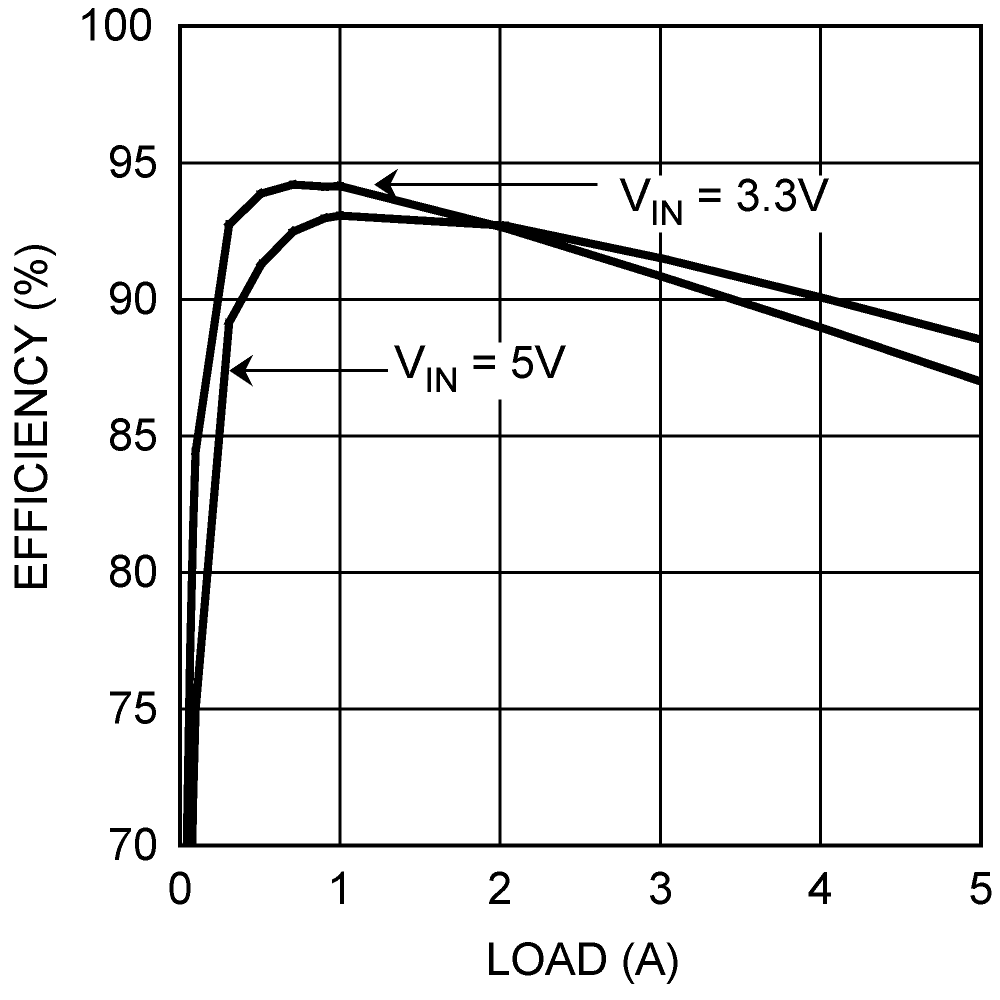
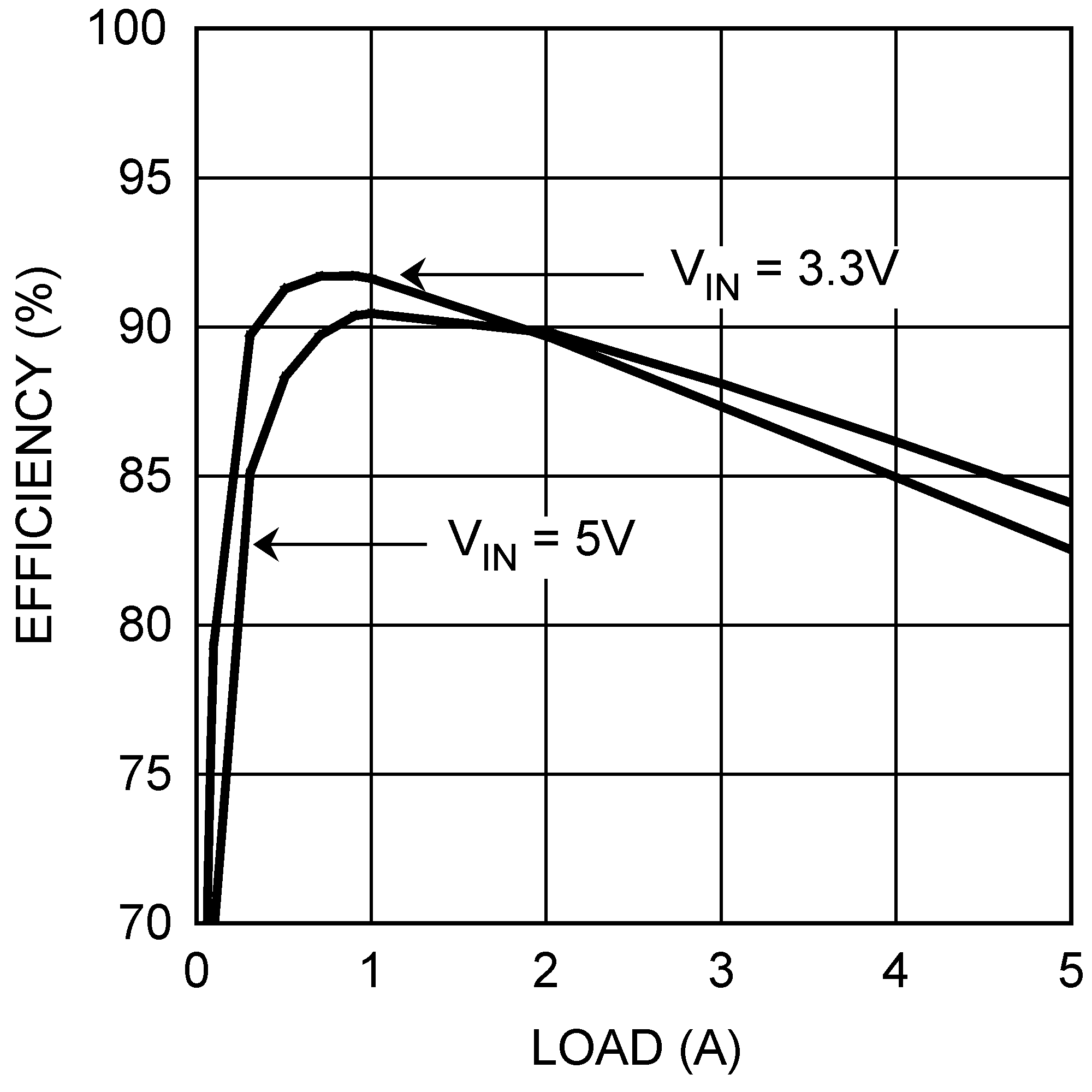
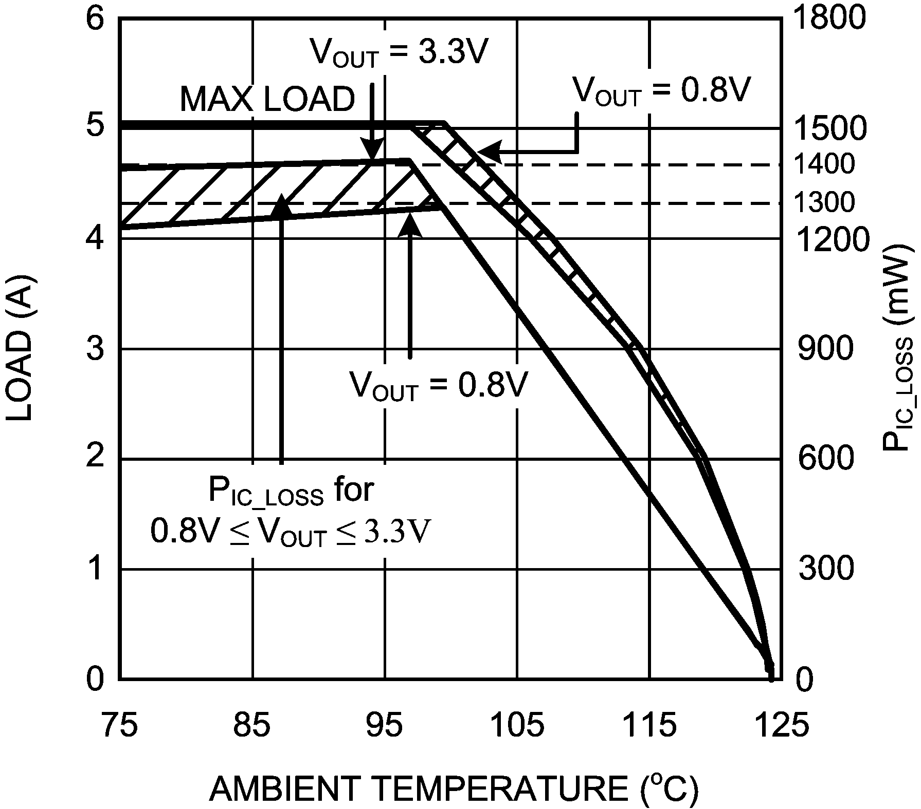
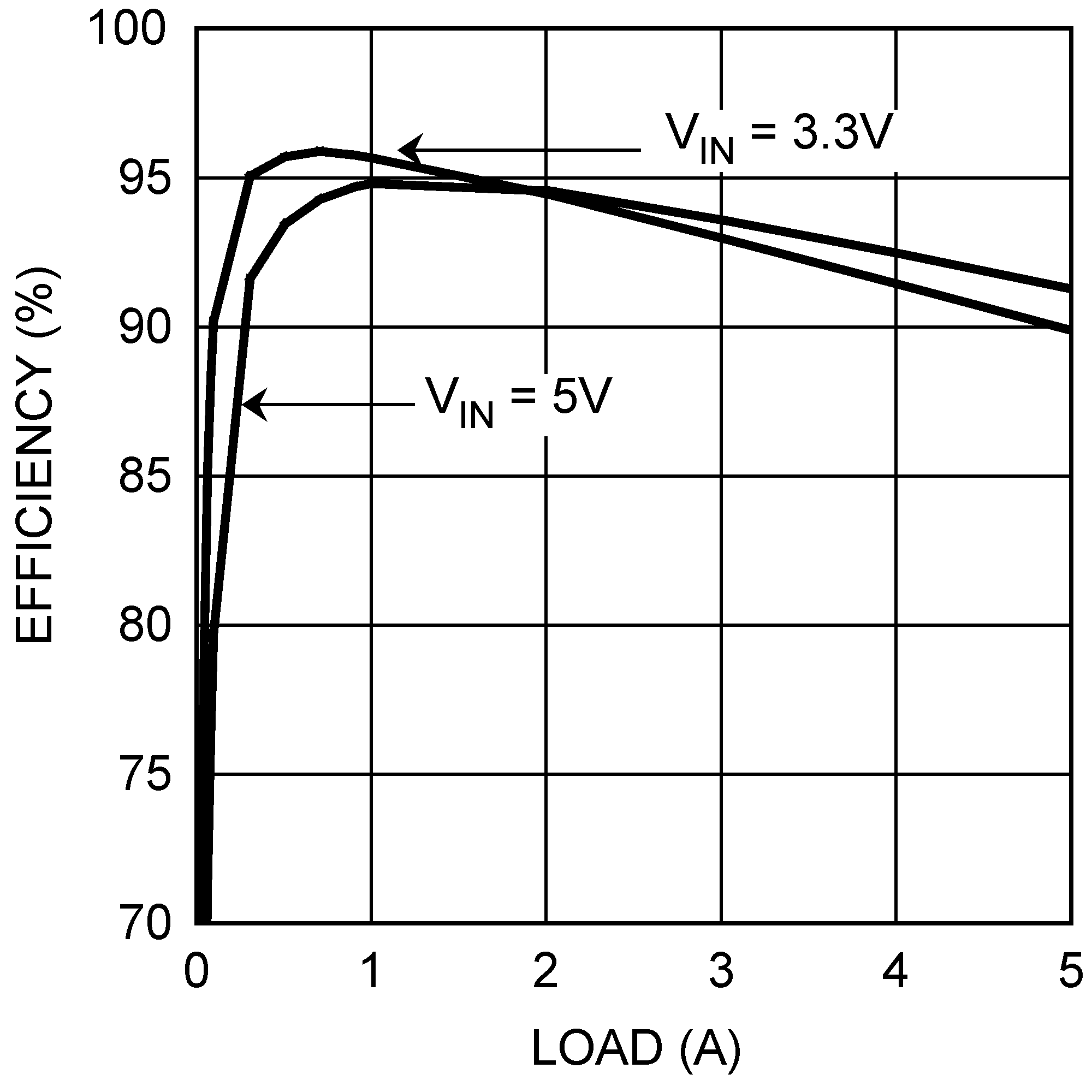
Unless otherwise specified, the following conditions apply: VIN = VEN = 5 V, CIN is 47-µF 10-V X5R ceramic capacitor; TA = 25°C for efficiency curves and waveforms.
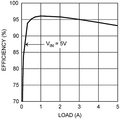
LMZ10505 30107471.png
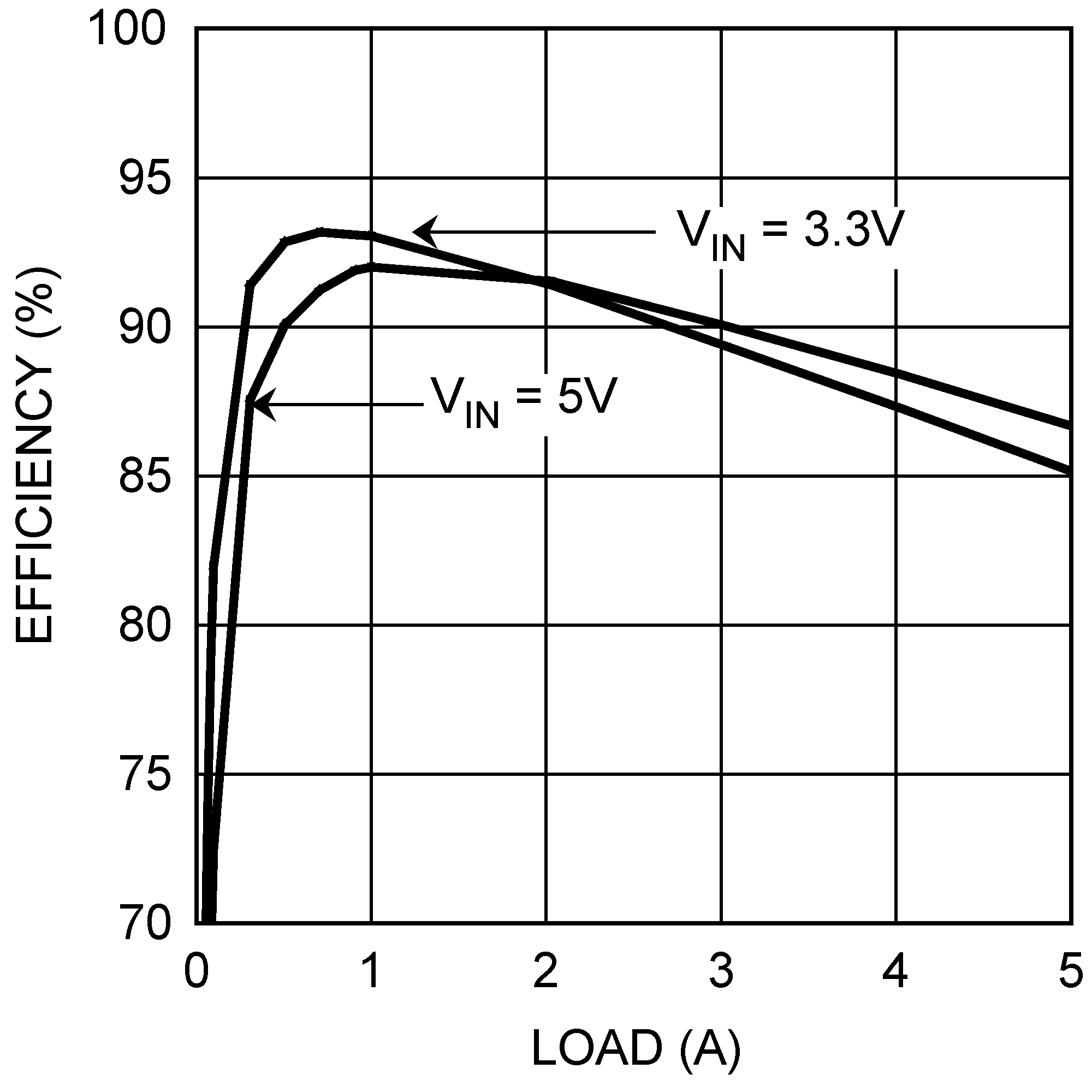
VOUT = 3.3 V
Figure 1. Efficiency
LMZ10505 30107469.png
VOUT = 1.8 V
Figure 3. Efficiency
LMZ10505 30107468.png
VOUT = 1.2 V
Figure 5. Efficiency
LMZ10505 30107414.png
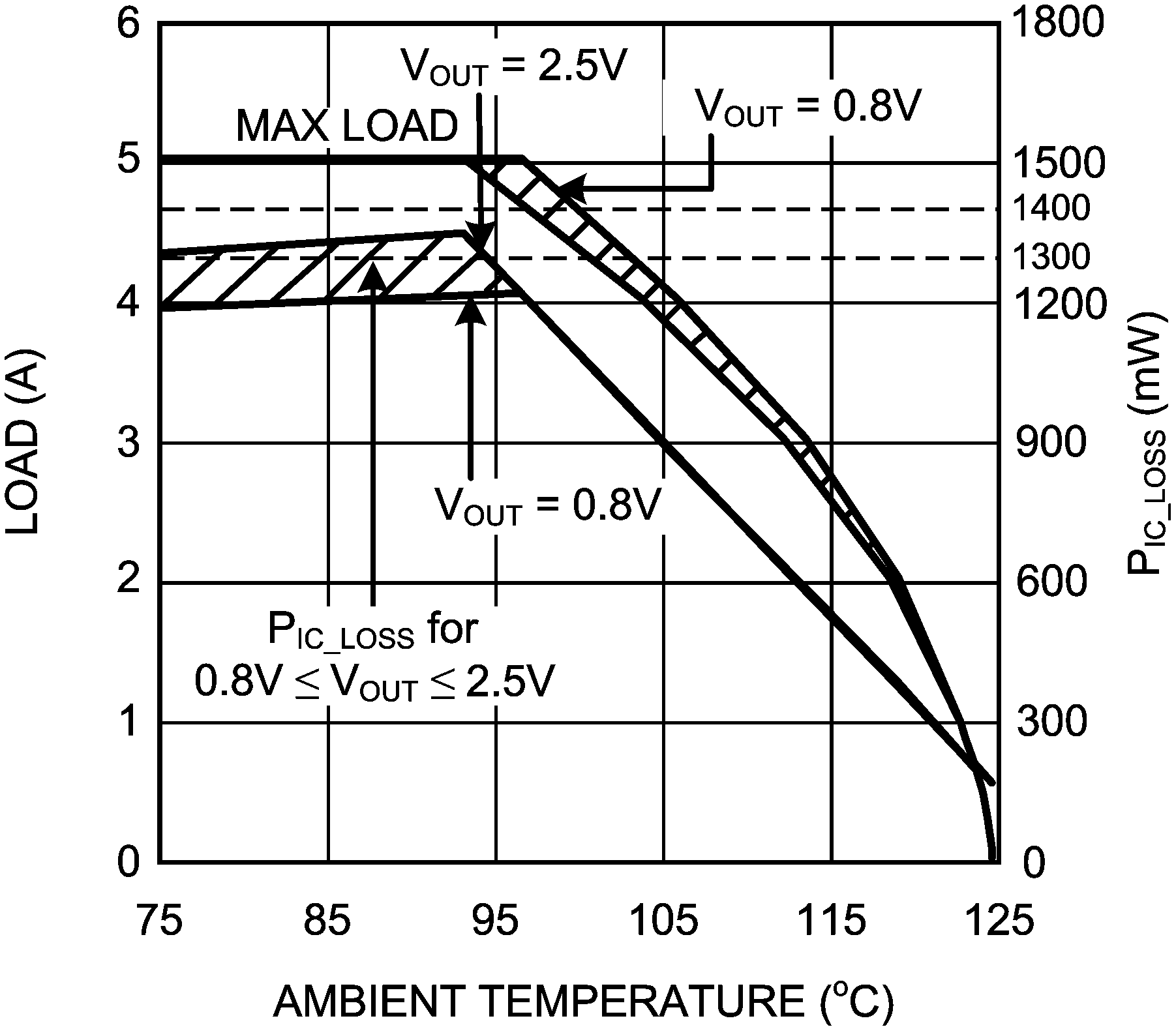
VIN = 5 V, θJA = 20°C/W
Figure 7. Current Derating
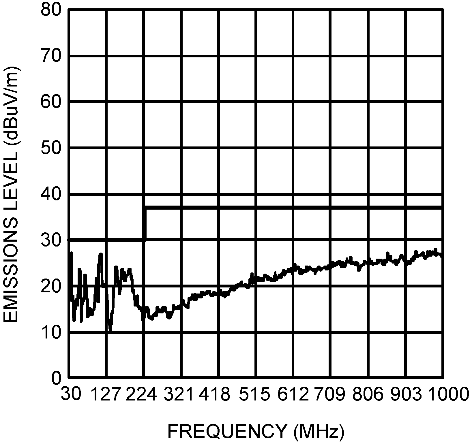
LMZ10505 30107412.png
VIN = 5 V, VOUT = 2.5 V, IOUT = 5 A Evaluation Board
Figure 9. Radiated Emissions (EN 55022, Class B)
LMZ10505 30107455.png
VOUT = 2.5 V, IOUT = 0 A
Figure 11. Prebiased Start-Up
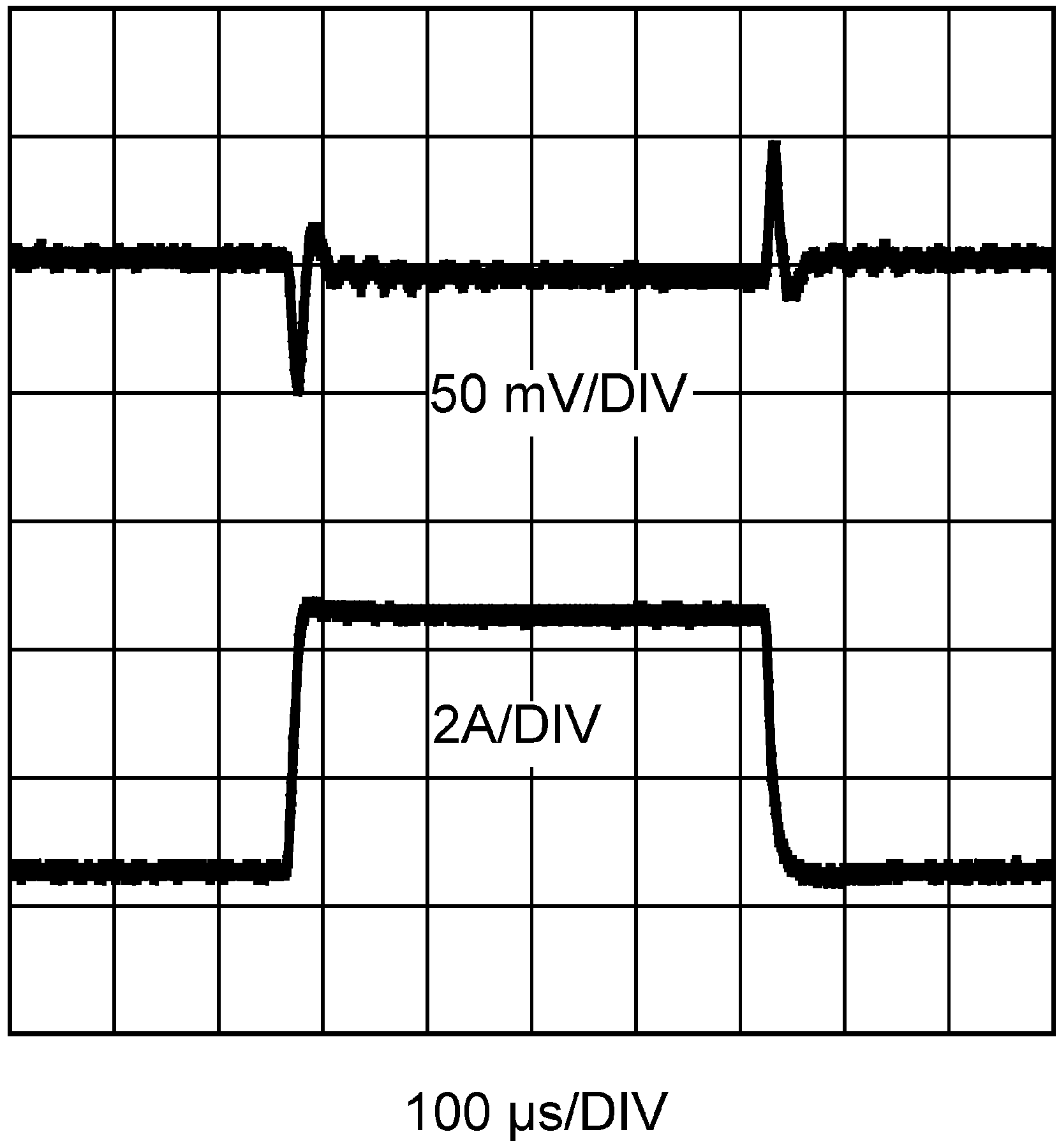
LMZ10505 30107463.png
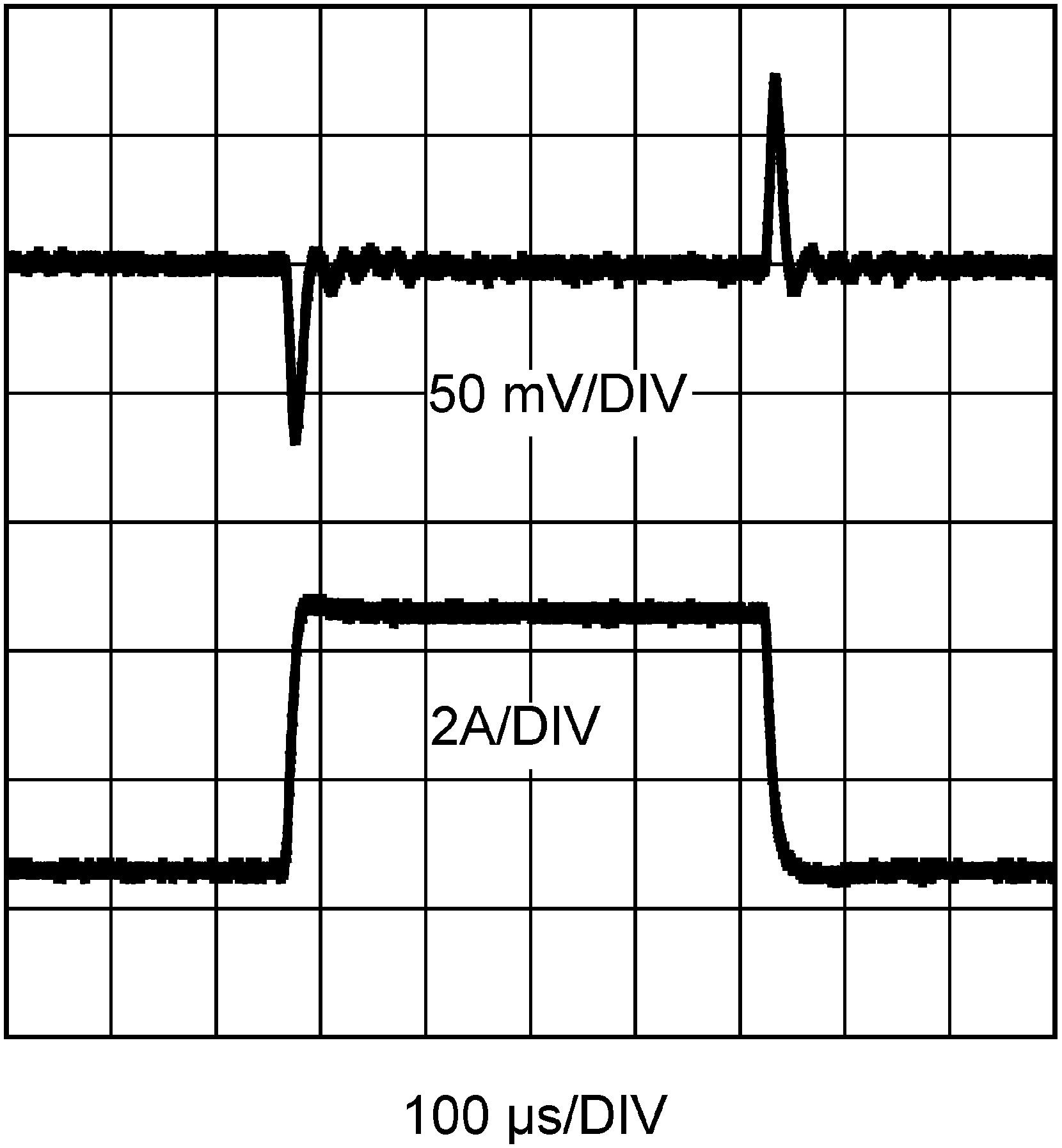
VIN = 5.0 V, VOUT = 2.5 V, IOUT = 0.5-A to 4.5-A to 0.5-A step
20-MHz Bandwidth Limited
Refer to Table 5 for BOM, includes optional components
Figure 13. Load Transient Response
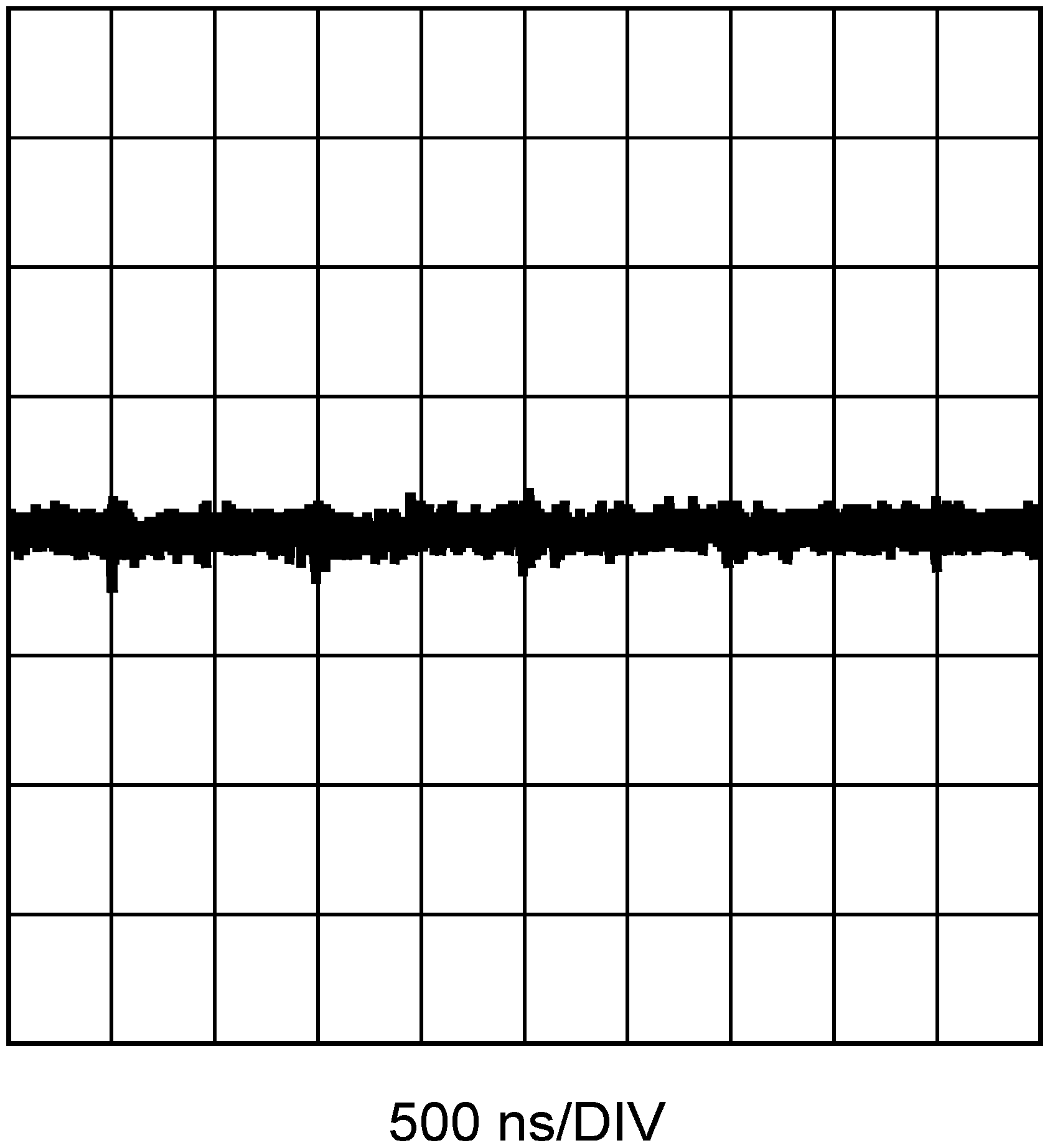
LMZ10505 30107465.png
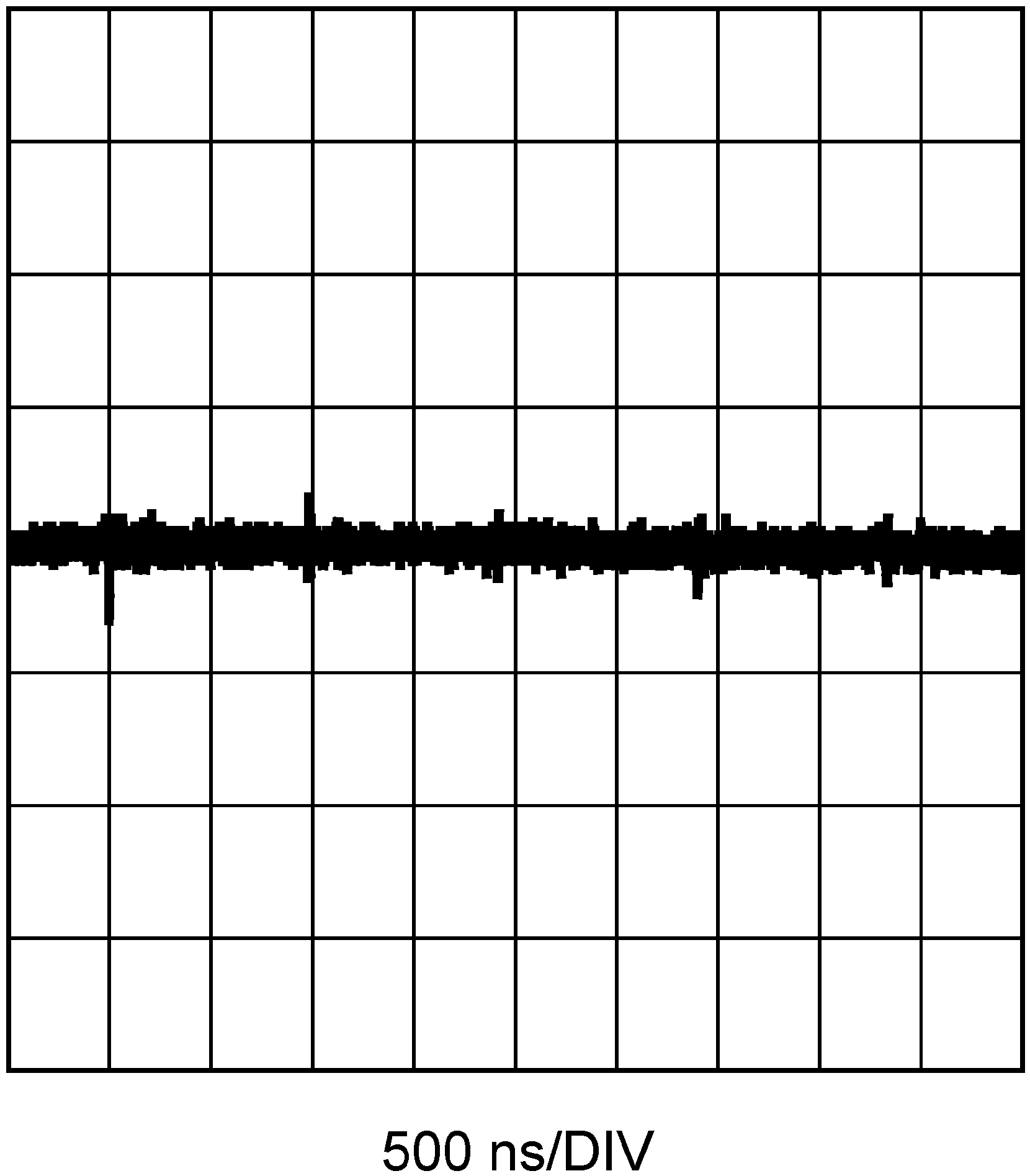
VIN = 5.0 V, VOUT = 2.5 V, IOUT = 5 A,
20 mV/DIV Refer to Table 5 for BOM
Figure 15. Output Voltage Ripple
LMZ10505 30107470.png
VOUT = 2.5 V
Figure 2. Efficiency
LMZ10505 30107411.png
VOUT = 1.5 V
Figure 4. Efficiency
LMZ10505 30107467.png
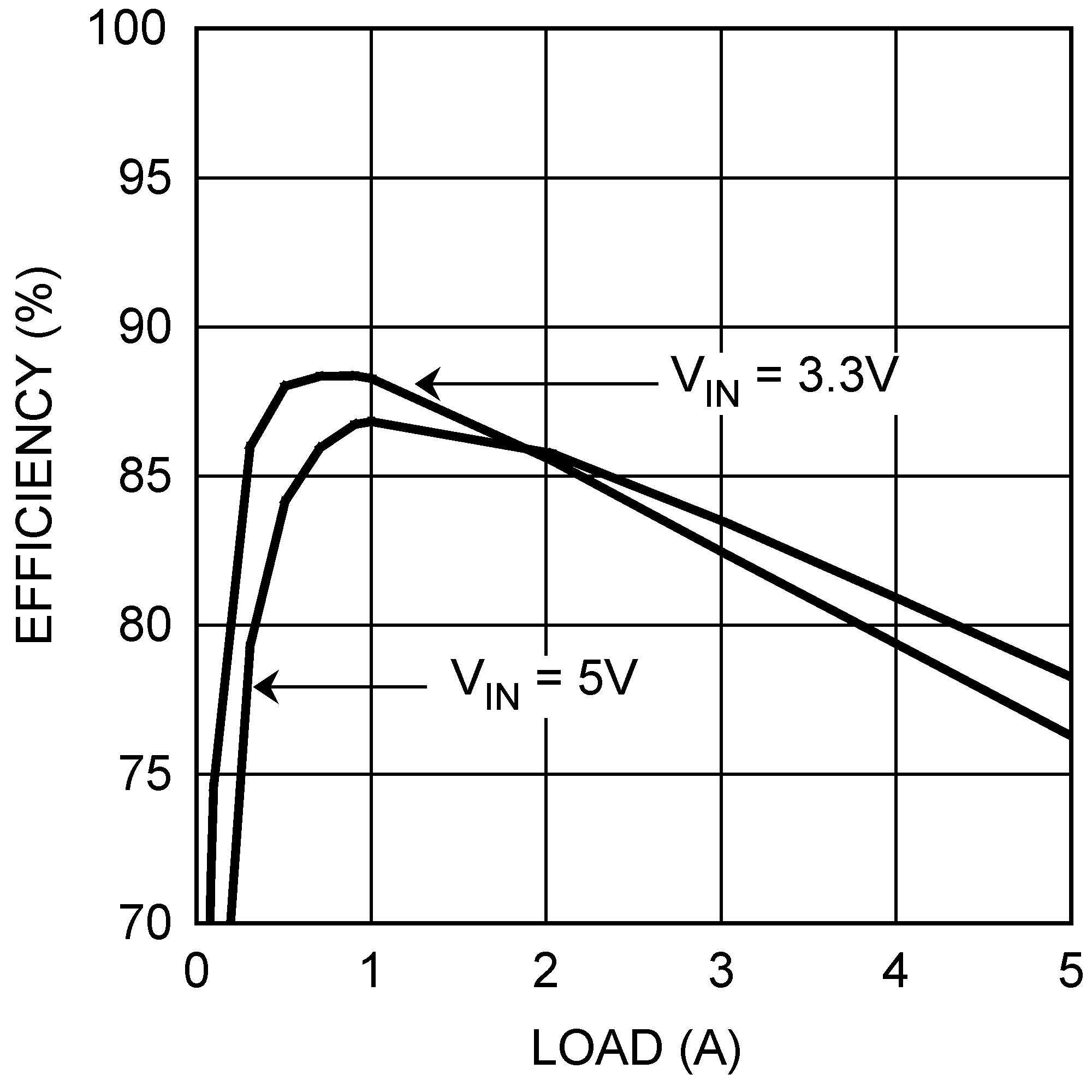
VOUT = 0.8 V
Figure 6. Efficiency
LMZ10505 30107415.png
VIN = 3.3 V, θJA = 20°C/W
Figure 8. Current Derating
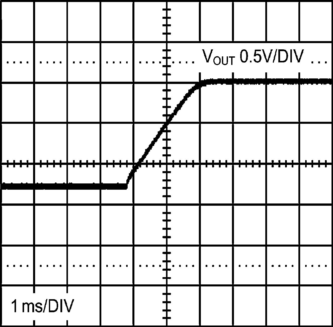
LMZ10505 30107456.png
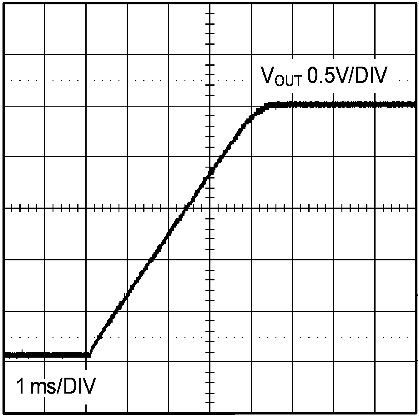
VOUT = 2.5 V, IOUT = 0 A
Figure 10. Start-Up
LMZ10505 30107462.png
VIN = 3.3 V, VOUT = 2.5 V, IOUT = 0.5-A to 4.5-A to 0.5-A step
20-MHz Bandwidth Limited
Refer to Table 5 for BOM, includes optional components
Figure 12. Load Transient Response
LMZ10505 30107464.png
VIN = 3.3 V, VOUT = 2.5 V, IOUT = 5 A, 20 mV/DIV
Refer to Table 5 for BOM
Figure 14. Output Voltage Ripple