ZHCSGT2C November   2016  – August 2021 LMS3635-Q1 , LMS3655-Q1

PRODUCTION DATA  

  1. 特性
  2. 应用
  3. 说明
  4. Revision History
  5. Device Comparison Tables
  6. Pin Configuration and Functions
  7. Specifications
    1. 7.1 Absolute Maximum Ratings
    2. 7.2 ESD Ratings
    3. 7.3 Recommended Operating Conditions
    4. 7.4 Thermal Information
    5. 7.5 Thermal Information (for Device Mounted on PCB)
    6. 7.6 Electrical Characteristics
    7. 7.7 System Characteristics
    8. 7.8 Timing Requirements
    9. 7.9 Typical Characteristics
  8. Detailed Description
    1. 8.1 Overview
    2. 8.2 Functional Block Diagram
      1. 8.2.1 Control Scheme
    3. 8.3 Feature Description
      1. 8.3.1 RESET Flag Output
      2. 8.3.2 Enable and Start-Up
      3. 8.3.3 Soft-Start Function
      4. 8.3.4 Current Limit
      5. 8.3.5 Hiccup Mode
      6. 8.3.6 Synchronizing Input
      7. 8.3.7 Undervoltage Lockout (UVLO) and Thermal Shutdown (TSD)
      8. 8.3.8 Input Supply Current
    4. 8.4 Device Functional Modes
      1. 8.4.1 AUTO Mode
      2. 8.4.2 FPWM Mode
      3. 8.4.3 Dropout
      4. 8.4.4 Spread-Spectrum Operation
  9. Application and Implementation
    1. 9.1 Application Information
    2. 9.2 Typical Applications
      1. 9.2.1 General Application
        1. 9.2.1.1 Design Requirements
        2. 9.2.1.2 Detailed Design Procedure
          1. 9.2.1.2.1 Custom Design With WEBENCH® Tools
          2. 9.2.1.2.2 External Components Selection
            1. 9.2.1.2.2.1 Input Capacitors
            2. 9.2.1.2.2.2 Output Inductors and Capacitors
              1. 9.2.1.2.2.2.1 Inductor Selection
              2. 9.2.1.2.2.2.2 Output Capacitor Selection
          3. 9.2.1.2.3 Setting the Output Voltage
          4. 9.2.1.2.4 FB for Adjustable Output
          5. 9.2.1.2.5 VCC
          6. 9.2.1.2.6 BIAS
          7. 9.2.1.2.7 CBOOT
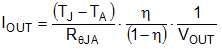
          8. 9.2.1.2.8 Maximum Ambient Temperature
        3. 9.2.1.3 Application Curves
      2. 9.2.2 Fixed 5-V Output for USB-Type Applications
        1. 9.2.2.1 Design Requirements
        2. 9.2.2.2 Detailed Design Procedure
        3. 9.2.2.3 Application Curves
      3. 9.2.3 Fixed 3.3-V Output
        1. 9.2.3.1 Design Requirements
        2. 9.2.3.2 Detailed Design Procedure
        3. 9.2.3.3 Application Curves
      4. 9.2.4 6-V Adjustable Output
        1. 9.2.4.1 Design Requirements
        2. 9.2.4.2 Detailed Design Procedure
        3. 9.2.4.3 Application Curves
    3. 9.3 Do's and Don't's
  10. 10Power Supply Recommendations
  11. 11Layout
    1. 11.1 Layout Guidelines
    2. 11.2 Layout Example
  12. 12Device and Documentation Support
    1. 12.1 Device Support
      1. 12.1.1 第三方产品免责声明
      2. 12.1.2 Development Support
        1. 12.1.2.1 Custom Design With WEBENCH® Tools
    2. 12.2 Documentation Support
      1. 12.2.1 Related Documentation
    3. 12.3 接收文档更新通知
    4. 12.4 支持资源
    5. 12.5 Trademarks
    6. 12.6 Electrostatic Discharge Caution
    7. 12.7 术语表
  13. 13Mechanical, Packaging, and Orderable Information

封装选项

机械数据 (封装 | 引脚)
散热焊盘机械数据 (封装 | 引脚)
订购信息
Maximum Ambient Temperature

As with any power conversion device, the LMS36x5-Q1 dissipates internal power while operating. The effect of this power dissipation is to raise the internal temperature of the converter above ambient. The internal die temperature (TJ) is a function of the ambient temperature, the power loss, and the effective thermal resistance, RθJA of the device and PCB combination. The maximum internal die temperature for the LMS3655-Q1 is 150°C, thus establishing a limit on the maximum device power dissipation and therefore load current at high ambient temperatures. Equation 5 shows the relationships between the important parameters.

Equation 5. GUID-7BF1CE84-B2F3-4507-9565-0E72B90747BE-low.gif

The device uses an advanced package technology that uses the pads and pins as heat spreading paths. As a result, the pads must be connected to large copper areas to dissipate the heat from the IC. All pins provide some heat relief capability but the PVINs, PGNDs, and SW pins are of particular importance for proper heat dissipation. Utilization of all the board layers for heat dissipation and using vias as heat pipes is recommended. The Section 11.1 includes an example that shows layout for proper heat management.