SNVSA10B November 2013 – November 2014 LMR14006
PRODUCTION DATA.
- 1 Features
- 2 Applications
- 3 Description
- 4 Revision History
- 5 Pin Configuration and Functions
- 6 Specifications
- 7 Detailed Description
- 8 Applications and Implementation
- 9 Layout
- 10Mechanical, Packaging, and Orderable Information
8 Applications and Implementation
NOTE
Information in the following applications sections is not part of the TI component specification, and TI does not warrant its accuracy or completeness. TI’s customers are responsible for determining suitability of components for their purposes. Customers should validate and test their design implementation to confirm system functionality.
8.1 Typical Applications
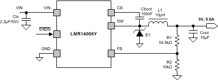 Figure 9. LMR14006 Design Example with 2.1 MHz Switching Frequency
Below are the recommended typical output voltage inductor/capacitor combinations for optimized total solution size.
| P/N | Vout(V) | R1(kΩ) | R2(kΩ) | L(μH) | Cout(μF) |
|---|---|---|---|---|---|
| LMR14006 Y | 5 | 54.9(1%) | 10(1%) | 3.3 | 22 |
| LMR14006 Y | 12 | 147(1%) | 10(1%) | 3.3 | 10 |
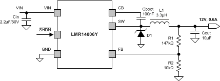 Figure 10. Application Circuit, 12 V Output
8.1.1 Design Requirements
This example details the design of a high frequency switching regulator using ceramic output capacitors. A few parameters must be known in order to start the design process. These parameters are typically determined at the system level:
Table 1. Design Parameters
| Input Voltage, VIN | 9V to 16V, Typical 12V | |
| Output Voltage, VOUT | 5.0V ± 3% | |
| Maximum Output Current IO_max | 0.6A | |
| Minimum Output Current IO_min | 0.03A | |
| Transient Response 0.03A to 0.6A | 5% | |
| Output Voltage Ripple | 1% | |
| Switching Frequency Fsw | 2.1MHz | |
| Target during Load Transient | Over Voltage Peak Value | 106% of Output Voltage |
| Under Voltage Value | 91% of Output Voltage | |
8.1.2 Detailed Design Procedure
8.1.2.1 Selecting The Switching Frequency
The first step is to decide on a switching frequency for the regulator. Typically, the user will want to choose the highest switching frequency possible since this will produce the smallest solution size. The high switching frequency allows for lower valued inductors and smaller output capacitors compared to a power supply that switches at a lower frequency. The switching frequency that can be selected is limited by the minimum on-time of the internal power switch, the input voltage and the output voltage and the frequency shift limitation. For this example, the output voltage is 5V and the maximum input voltage is 16 V, a switching frequency of 2100 kHz is used.
8.1.2.2 Output Inductor Selection
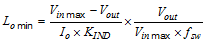
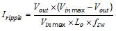
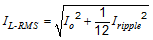
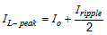
The most critical parameters for the inductor are the inductance, peak current and the DC resistance. The inductance is related to the peak-to-peak inductor ripple current, the input and the output voltages. Since the ripple current increases with the input voltage, the maximum input voltage is always used to determine the inductance. To calculate the minimum value of the output inductor, use Equation 1. KIND is a coefficient that represents the amount of inductor ripple current relative to the maximum output current. A reasonable value is setting the ripple current to be 30% of the DC output current. For this design example, the minimum inductor value is calculated to be 9.1 µH, and a nearest standard value was chosen: 10 µH. For the output filter inductor, it is important that the RMS current and saturation current ratings not be exceeded. The RMS and peak inductor current can be found from Equation 3 and Equation 4. The inductor ripple current is 0.16 A, and the RMS current is 0.602 A. As the equation set demonstrates, lower ripple currents will reduce the output voltage ripple of the regulator but will require a larger value of inductance. A good starting point for most applications is a 10 μH with 2 A current rating. Using a rating near 2 A will enable the LMR14006 to current limit without saturating the inductor. This is preferable to the LMR14006 going into thermal shutdown mode and the possibility of damaging the inductor if the output is shorted to ground or other long-term overload.
8.1.2.3 Output Capacitor
The selection of COUT is mainly driven by three primary considerations. The output capacitor will determine the modulator pole, the output voltage ripple, and how the regulator responds to a large change in load current. The output capacitance needs to be selected based on the most stringent of these three criteria.
The desired response to a large change in the load current is the first criteria. The regulator usually needs two or more clock cycles for the control loop to see the change in load current and output voltage and adjust the duty cycle to react to the change. The output capacitance must be large enough to supply the difference in current for 2 clock cycles while only allowing a tolerable amount of droop in the output voltage. Equation 5 shows the minimum output capacitance necessary to accomplish this. For this example, the transient load response is specified as a 3% change in VOUT for a load step from 0.03A to 0.6A (full load). For this example, ΔIOUT = 0.6 -0.03 = 0.57 A and ΔVOUT = 0.03 × 5 = 0.15 V. Using these numbers gives a minimum capacitance of 3.6µF. For ceramic capacitors, the ESR is usually small enough to ignore in this calculation. Aluminum electrolytic and tantalum capacitors have higher ESR that should be taken into account.
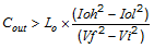
The stored energy in the inductor will produce an output voltage overshoot when the load current rapidly decreases. The output capacitor must also be sized to absorb energy stored in the inductor when transitioning from a high load current to a lower load current. Equation 6 is used to calculate the minimum capacitance to keep the output voltage overshoot to a desired value. Where L is the value of the inductor, IOH is the output current under heavy load, IOL is the output under light load, Vf is the final peak output voltage, and Vi is the initial capacitor voltage. For this example, the worst case load step will be from 0.6 A to 0.03 A. The output voltage will increase during this load transition and the stated maximum in our specification is 3% of the output voltage. This will make Vo_overshoot = 1.03 × 5 = 5.15 V. Vi is the initial capacitor voltage which is the nominal output voltage of 5V. Using these numbers in Equation 6 yields a minimum capacitance of 2.36 µF.
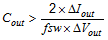
Equation 7 calculates the minimum output capacitance needed to meet the output voltage ripple specification. Where fsw is the switching frequency, Vo_ripple is the maximum allowable output voltage ripple, and IL_ripple is the inductor ripple current. Equation 7 yields 0.21µF.
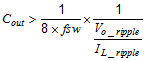
Equation 8 calculates the maximum ESR an output capacitor can have to meet the output voltage ripple specification. Equation 8 indicates the ESR should be less than 277mΩ.
Additional capacitance de-ratings for aging, temperature and dc bias should be factored in which will increase this minimum value. For this example, 10µF ceramic capacitors will be used. Capacitors in the range of 4.7µF-100µF are a good starting point with an ESR of 0.1Ω or less.

8.1.2.4 Schottky Diode
The breakdown voltage rating of the diode is preferred to be 25% higher than the maximum input voltage. The current rating for the diode should be equal to the maximum output current for best reliability in most applications. In cases where the input voltage is much greater than the output voltage the average diode current is lower. In this case it is possible to use a diode with a lower average current rating, approximately (1-D) × IOUT however the peak current rating should be higher than the maximum load current. A 0.5A to 1A rated diode is a good starting point.
8.1.2.5 Input Capacitor
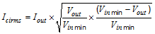
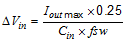
A low ESR ceramic capacitor is needed between the VIN pin and ground pin. This capacitor prevents large voltage transients from appearing at the input. Use a 1µF-10µF value with X5R or X7R dielectric. Depending on construction, a ceramic capacitor’s value can decrease up to 50% of its nominal value when rated voltage is applied. Consult with the capacitor manufactures data sheet for information on capacitor derating over voltage and temperature. The capacitor must also have a ripple current rating greater than the maximum input current ripple of the LMR14006. The input ripple current can be calculated using below Equation 9.
For this example design, one 2.2µF, 50V capacitor is selected. The input capacitance value determines the input ripple voltage of the regulator. The input voltage ripple can be calculated using Equation 10. Using the design example values, IOUTmax = 0.6A, CIN = 2.2µF, ƒSW = 2100kHz, yields an input voltage ripple of 32.5mV and a rms input ripple current of 0.3A.
8.1.2.6 Bootstrap Capacitor Selection
A 0.1μF ceramic capacitor or larger is recommended for the bootstrap capacitor (CBOOT). For applications where the input voltage is close to output voltage a larger capacitor is recommended, generally 0.1 µF to 1 µF to ensure plenty of gate drive for the internal switches and a consistently low RDSON. A ceramic capacitor with an X7R or X5R grade dielectric with a voltage rating of 10V or higher is recommended because of the stable characteristics over temperature and voltage.
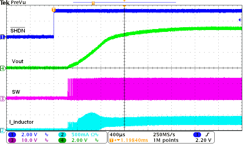
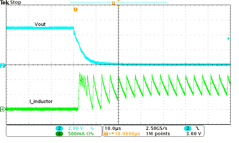
8.1.3 Application Performance Curves
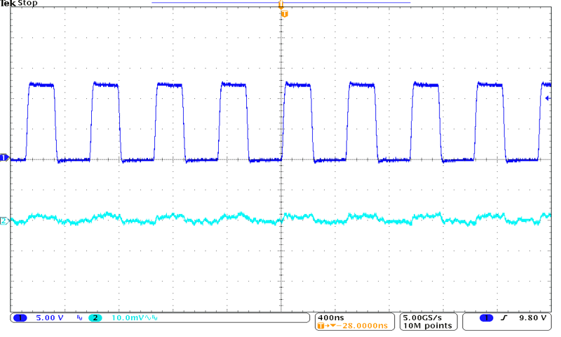
| Vout = 5 V | 600 mA Load | |
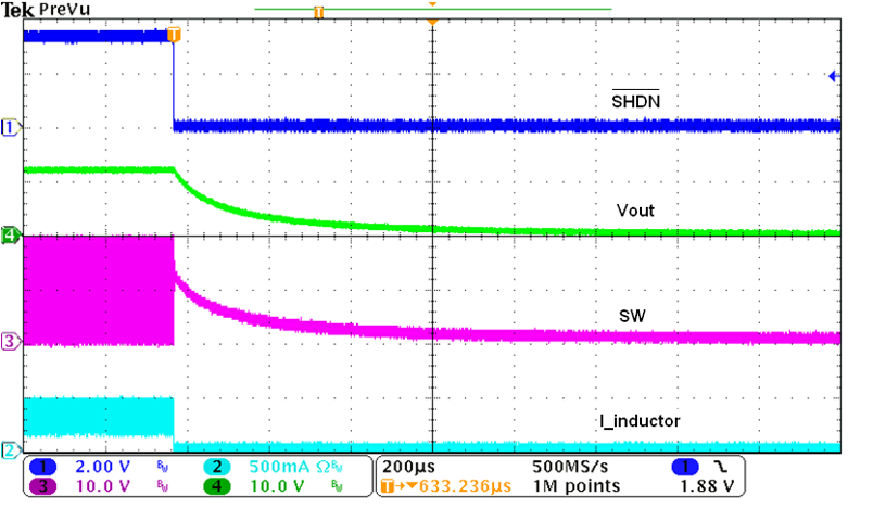
| Vin = 18 V | 300 mA Load | |
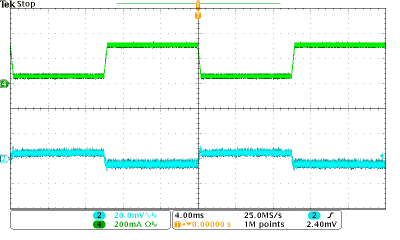
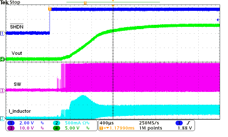
| Vin = 18V | 300 mA Load | |