ZHCSA23B September 2011 – June 2019 LMR12010
PRODUCTION DATA.
- 1 特性
- 2 应用
- 3 说明
- 4 修订历史记录
- 5 Pin Configuration and Functions
- 6 Specifications
- 7 Detailed Description
- 8 Application and Implementation
- 9 Layout
- 10器件和文档支持
- 11机械、封装和可订购信息
请参考 PDF 数据表获取器件具体的封装图。
机械数据 (封装 | 引脚)
- DDC|6
散热焊盘机械数据 (封装 | 引脚)
7.1 Overview
The LMR12010 is a constant frequency PWM buck regulator IC that delivers a 1-A load current. The regulator has a preset switching frequency of either 3 MHz (LMR12010Y) or 1.6 MHz (LMR12010X). These high frequencies allow the LMR12010 to operate with small surface mount capacitors and inductors, resulting in DC/DC converters that require a minimum amount of board space. The LMR12010 is internally compensated, so it is simple to use, and requires few external components. The LMR12010 uses current-mode control to regulate the output voltage.
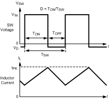
The following operating description of the LMR12010 refers to the functional block diagram (Functional Block Diagram) and to the waveforms in Figure 14. The LMR12010 supplies a regulated output voltage by switching the internal NMOS control switch at constant frequency and variable duty cycle. A switching cycle begins at the falling edge of the reset pulse generated by the internal oscillator. When this pulse goes low, the output control logic turns on the internal NMOS control switch. During this on-time, the SW pin voltage (VSW) swings up to approximately VIN, and the inductor current (IL) increases with a linear slope. IL is measured by the current-sense amplifier, which generates an output proportional to the switch current. The sense signal is summed with the regulator’s corrective ramp and compared to the error amplifier’s output, which is proportional to the difference between the feedback voltage and VREF. When the PWM comparator output goes high, the output switch turns off until the next switching cycle begins. During the switch off-time, inductor current discharges through Schottky diode D1, which forces the SW pin to swing below ground by the forward voltage (VD) of the catch diode. The regulator loop adjusts the duty cycle (D) to maintain a constant output voltage.
 Figure 14. LMR12010 Waveforms Of SW Pin Voltage and Inductor Current