SNOSAW6E January 2008 – December 2014 LMP7721
PRODUCTION DATA.
- 1 Features
- 2 Applications
- 3 Description
- 4 Revision History
- 5 Pin Configuration and Functions
- 6 Specifications
- 7 Detailed Description
- 8 Application and Implementation
- 9 Power Supply Recommendations
- 10Layout
- 11Device and Documentation Support
- 12Mechanical, Packaging, and Orderable Information
10 Layout
10.1 Layout Guidelines
In order to capitalize on the LMP7721’s ultra-low input bias current, careful circuit layout and assembly are required. Guarding techniques are highly recommended to reduce parasitic leakage current by isolating the LMP7721’s input from large voltage gradients across the PC board. A guard is a low-impedance conductor that surrounds an input line and its potential is raised to the input line’s voltage. The input pins should be fully guarded as shown in Figure 54. The guard traces should completely encircle the input connections. In addition, they should be located on both sides of the PCB and be connected together.
To further guard the inputs from the supply pins, the two N/C pins may be connected to the guard trace which will provide guarding down to the leadframe level.
Solder mask should not cover the input and the guard area including guard traces on either side of the PCB.
Keep switching power supplies and other noise-producing devices away from the input area.
10.2 Layout Example
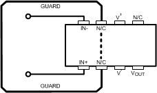 Figure 54. Layout Example Showing Guard Trace