SNOSA83I August 2003 – August 2014 LMH6723 , LMH6724
PRODUCTION DATA.
- 1 Features
- 2 Applications
- 3 Description
- 4 Revision History
- 5 Pin Configuration and Functions
- 6 Specifications
- 7 Application and Implementation
- 8 Power Supply Recommendations
- 9 Device and Documentation Support
- 10Mechanical, Packaging, and Orderable Information
封装选项
机械数据 (封装 | 引脚)
散热焊盘机械数据 (封装 | 引脚)
订购信息
6 Specifications
6.1 Absolute Maximum Ratings(2)(6)(1)
over operating free-air temperature range (unless otherwise noted)| MIN | MAX | UNIT | ||
|---|---|---|---|---|
| VCC (V+ - V-) | ±6.75 | V | ||
| IOUT | 120(4) | mA | ||
| Common Mode Input Voltage | ±VCC | V | ||
| Maximum Junction Temperature | +150 | °C | ||
| Soldering Information | Infrared or Convection (20 sec) | 235 | °C | |
| Wave Soldering (10 sec) | 260 | °C | ||
6.2 Handling Ratings
| MIN | MAX | UNIT | |||
|---|---|---|---|---|---|
| Tstg | Storage temperature range | −65 | +150 | °C | |
| V(ESD) | Electrostatic discharge | Human body model (HBM), per ANSI/ESDA/JEDEC JS-001, all pins(1)(5) | 2000 | V | |
| Machine Model (MM), per JEDEC specification JESD22-C101, all pins(5)(2) | 200 | ||||
(1) JEDEC document JEP155 states that 2000-V HBM allows safe manufacturing with a standard ESD control process.
(2) JEDEC document JEP157 states that 200-V MM allows safe manufacturing with a standard ESD control process.
6.3 Recommended Operating Conditions(4)
over operating free-air temperature range (unless otherwise noted)| MIN | NOM | MAX | UNIT | |
|---|---|---|---|---|
| Operating Temperature Range | −40 | +85 | °C | |
| Nominal Supply Voltage | 4.5 | 12 | V |
6.4 Thermal Information
| THERMAL METRIC(1) | SOT-23 | SOIC | UNIT | |
|---|---|---|---|---|
| DBV | D08A | |||
| 5 PINS | 8 PINS | |||
| RθJA | Junction-to-ambient thermal resistance | 230°C/W | 166°C/W | °C/W |
(1) For more information about traditional and new thermal metrics, see the IC Package Thermal Metrics application report, SPRA953.
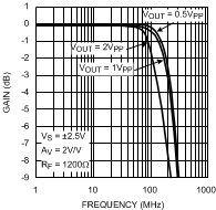
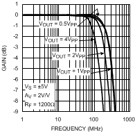
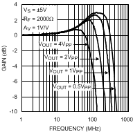
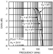
6.5 ±5V Electrical Characteristics
Unless otherwise specified, AV = +2, RF = 1200Ω, RL = 100Ω. Boldface limits apply at temperature extremes.(3)| PARAMETER | TEST CONDITIONS | MIN | TYP | MAX | UNIT | ||
|---|---|---|---|---|---|---|---|
| FREQUENCY DOMAIN RESPONSE | |||||||
| SSBW | −3 dB Bandwidth Small Signal | VOUT = 0.5 VPP | 260 | MHz | |||
| LSBW | −3dB Bandwidth Large Signal | VOUT = 4.0 VPP | 90 | 110 | MHz | ||
| 85 | 95 | ||||||
| UGBW | −3 dB Bandwidth Unity Gain | VOUT = .2 VPP AV = 1 V/V | 370 | MHz | |||
| .1dB BW | .1 dB Bandwidth | VOUT = 0.5 VPP | 100 | MHz | |||
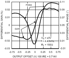
| DG | Differential Gain | RL = 150Ω, 4.43 MHz | 0.03% | ||||
| DP | Differential Phase | RL = 150Ω, 4.43 MHz | 0.11 | deg | |||
| TIME DOMAIN RESPONSE | |||||||
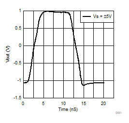
| TRS | Rise and Fall Time | 4V Step | 2.5 | ns | |||
| TSS | Settling Time to 0.05% | 2V Step | 30 | ns | |||
| SR | Slew Rate | 4V Step | 500 | 600 | V/μs | ||
| DISTORTION and NOISE RESPONSE | |||||||
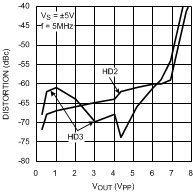
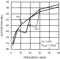
| HD2 | 2nd Harmonic Distortion | 2 VPP, 5 MHz | −65 | dBc | |||
| HD3 | 3rd Harmonic Distortion | 2 VPP, 5 MHz | −63 | dBc | |||
| EQUIVALENT INPUT NOISE | |||||||
| VN | Non-Inverting Voltage Noise | >1 MHz | 4.3 | nV/√Hz | |||
| NICN | Inverting Current Noise | >1 MHz | 6 | pA/√Hz | |||
| ICN | Non-Inverting Current Noise | >1 MHz | 6 | pA/√Hz | |||
| STATIC, DC PERFORMANCE | |||||||
| VIO | Input Offset Voltage | 1 | ±3 ±3.7 |
mV | |||
| IBN | Input Bias Current | Non-Inverting | −2 | ±4 ±5 |
µA | ||
| IBI | Input Bias Current | Inverting | 0.4 | ±4 ±5 |
µA | ||
| PSRR | Power Supply Rejection Ratio | DC, 1V Step | LMH6723 | 59 57 |
64 | dB | |
| LMH6724 | 59 55 |
64 | |||||
| CMRR | Common Mode Rejection Ratio | DC, 1V Step | LMH6723 | 57 55 |
60 | dB | |
| LMH6724 | 57 53 |
60 | |||||
| ICC | Supply Current (per amplifier) | RL = ∞ | 1 | 1.2 1.4 |
mA | ||
| MISCELLANEOUS PERFORMANCE | |||||||
| RIN+ | Input Resistance | Non-Inverting | 100 | kΩ | |||
| RIN− | Input Resistance (Output Resistance of Input Buffer) |
Inverting | 500 | Ω | |||
| CIN | Input Capacitance | Non-Inverting | 1.5 | pF | |||
| ROUT | Output Resistance | Closed Loop | 0.01 | Ω | |||
| VO | Output Voltage Range | RL = ∞ | LMH6723 | ±4 ±3.9 |
±4.1 | V | |
| LMH6724 | ±4 ±3.85 |
±4.1 | |||||
| VOL | Output Voltage Range, High | RL = 100Ω | 3.6 3.5 |
3.7 | V | ||
| Output Voltage Range, Low | RL = 100Ω | −3.25 −3.1 |
−3.45 | ||||
| CMVR | Input Voltage Range | Common Mode, CMRR > 50 dB | ±4.0 | V | |||
| IO | Output Current | Sourcing, VOUT = 0 | 95 70 |
110 | mA | ||
| Sinking, VOUT = 0 | −80 −70 |
110 | |||||
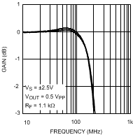
6.6 ±2.5V Electrical Characteristics
Unless otherwise specified, AV = +2, RF = 1200Ω, RL = 100Ω. Boldface limits apply at temperature extremes.(3)| PARAMETER | TEST CONDITIONS | MIN | TYP | MAX | UNIT | ||
|---|---|---|---|---|---|---|---|
| FREQUENCY DOMAIN RESPONSE | |||||||
| SSBW | −3 dB Bandwidth Small Signal | VOUT = 0.5 VPP | 210 | MHz | |||
| LSBW | −3 dB Bandwidth Large Signal | VOUT = 2.0 VPP | 95 | 125 | MHz | ||
| UGBW | −3 dB Bandwidth Unity Gain | VOUT = 0.5 VPP, AV = 1 V/V | 290 | MHz | |||
| .1dB BW | .1 dB Bandwidth | VOUT = 0.5 VPP | 100 | MHz | |||
| DG | Differential Gain | RL = 150Ω, 4.43 MHz | .03% | ||||
| DP | Differential Phase | RL = 150Ω, 4.43 MHz | 0.1 | deg | |||
| TIME DOMAIN RESPONSE | |||||||
| TRS | Rise and Fall Time | 2V Step | 4 | ns | |||
| SR | Slew Rate | 2V Step | 275 | 400 | V/μs | ||
| DISTORTION AND NOISE RESPONSE | |||||||
| HD2 | 2nd Harmonic Distortion | 2 VPP, 5 MHz | −67 | dBc | |||
| HD3 | 3rd Harmonic Distortion | 2 VPP, 5 MHz | −67 | dBc | |||
| EQUIVALENT INPUT NOISE | |||||||
| VN | Non-Inverting Voltage | >1 MHz | 4.3 | nV/√Hz | |||
| NICN | Inverting Current | >1MHz | 6 | pA/√Hz | |||
| ICN | Non-Inverting Current | >1MHz | 6 | pA/√Hz | |||
| STATIC, DC PERFORMANCE | |||||||
| VIO | Input Offset Voltage | −0.5 | ±3 ±3.4 |
mV | |||
| IBN | Input Bias Current | Non-Inverting | −2.7 | ±4 ±5 |
µA | ||
| IBI | Input Bias Current | Inverting | −0.7 | ±4 ±5 |
µA | ||
| PSRR | Power Supply Rejection Ratio | DC, 0.5V Step | LMH6723 | 59 57 |
62 | dB | |
| LMH6724 | 58 55 |
62 | |||||
| CMRR | Common Mode Rejection Ratio | DC, 0.5V Step | LMH6723 | 57 53 |
59 | dB | |
| LMH6724 | 55 52 |
59 | |||||
| ICC | Supply Current (per amplifier) | RL = ∞ | 0.9 | 1.1 1.3 |
mA | ||
| MISCELLANEOUS PERFORMANCE | |||||||
| RIN+ | Input Resistance | Non-Inverting | 100 | kΩ | |||
| RIN− | Input Resistance (Output Resistance of Input Buffer) |
Inverting | 500 | Ω | |||
| CIN | Input Capacitance | Non-Inverting | 1.5 | pF | |||
| ROUT | Output Resistance | Closed Loop | 0.02 | Ω | |||
| VO | Output Voltage Range | RL = ∞ | ±1.55 ±1.4 |
±1.65 | V | ||
| VOL | Output Voltage Range, High | RL = 100Ω | LMH6723 | 1.35 1.27 |
1.45 | V | |
| LMH6724 | 1.35 1.26 |
1.45 | |||||
| Output Voltage Range, Low | RL = 100Ω | LMH6723 | −1.25 −1.15 |
−1.38 | V | ||
| LMH6724 | −1.25 −1.15 |
−1.38 | |||||
| CMVR | Input Voltage Range | Common Mode, CMRR > 50 dB | ±1.45 | V | |||
| IO | Output Current | Sourcing | 70 60 |
90 | mA | ||
| Sinking | −30 −30 |
−60 | |||||
(1) Stresses beyond those listed under Absolute Maximum Ratings may cause permanent damage to the device. These are stress ratings only, which do not imply functional operation of the device at these or any other conditions beyond those indicated under Recommended Operating Conditions. Exposure to absolute-maximum-rated conditions for extended periods may affect device reliability.
(2) Absolute Maximum Ratings indicate limits beyond which damage to the device may occur. Operating Ratings indicate conditions for which the device is intended to be functional, but specific performance is not ensured. For ensured specifications, see the Electrical Characteristics tables.
(3) Electrical Table values apply only for factory testing conditions at the temperature indicated. Factory testing conditions result in very limited self-heating of the device such that TJ = TA. No ensured specification of parametric performance is indicated in the electrical tables under conditions of internal self heating where TJ > TA. See Application and Implementation for information on temperature derating of this device. Min/Max ratings are based on product characterization and simulation. Individual parameters are tested as noted.
(4) The maximum continuous output current (IOUT) is determined by device power dissipation limitations. See Power Supply Recommendations for more details.
(5) Human Body Model, 1.5 kΩ in series with 100 pF. Machine Model, 0Ω In series with 200 pF.
(6) If Military/Aerospace specified devices are required, please contact the Texas Instruments Sales Office/Distributors for availability and specifications.
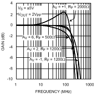
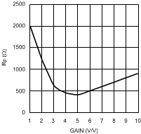
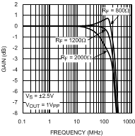
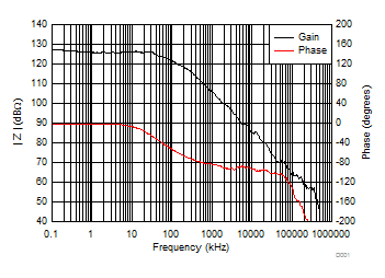
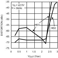
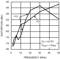
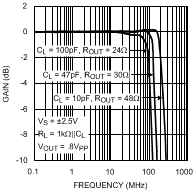
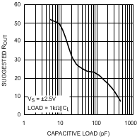
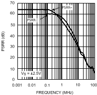
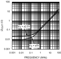
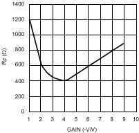
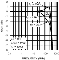
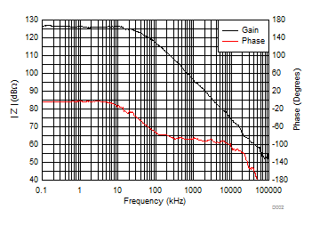
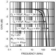
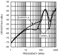
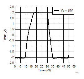
6.7 Typical Performance Characteristics
AV = 2, RF = 1200Ω, RL = 100Ω, unless otherwise specified.