SNOSA35G August   2002  – July 2015 LMH6657 , LMH6658

PRODUCTION DATA.  

  1. Features
  2. Applications
  3. Description
  4. Revision History
  5. Pin Configuration and Functions
  6. Specifications
    1. 6.1 Absolute Maximum Ratings
    2. 6.2 ESD Ratings
    3. 6.3 Recommended Operating Conditions
    4. 6.4 Thermal Information
    5. 6.5 Electrical Characteristics, 5 V
    6. 6.6 Electrical Characteristics, ±5 V
    7. 6.7 Typical Characteristics
  7. Detailed Description
    1. 7.1 Overview
      1. 7.1.1 Large Signal Behavior
    2. 7.2 Feature Description
    3. 7.3 Device Functional Modes
      1. 7.3.1 Output Phase Reversal
  8. Application and Implementation
    1. 8.1 Application Information
      1. 8.1.1 Output Characteristics
        1. 8.1.1.1 Output Current Capability
        2. 8.1.1.2 Driving Capacitive Loads
        3. 8.1.1.3 Distortion
  9. Power Supply Recommendations
  10. 10Layout
    1. 10.1 Layout Guidelines
    2. 10.2 Layout Example
  11. 11Device and Documentation Support
    1. 11.1 Documentation Support
      1. 11.1.1 Related Documentation
    2. 11.2 Related Links
    3. 11.3 Community Resources
    4. 11.4 Trademarks
    5. 11.5 Electrostatic Discharge Caution
    6. 11.6 Glossary
  12. 12Mechanical, Packaging, and Orderable Information

封装选项

机械数据 (封装 | 引脚)
散热焊盘机械数据 (封装 | 引脚)
订购信息

5 Pin Configuration and Functions

DBV and DCK Package
5-Pin SOT-23 and SC70
Top View
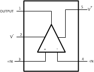
LMH6657 LMH6658 20053261.gif
D and DGK Package
8-Pin SOIC and VSSOP
Top View
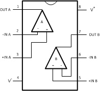
LMH6657 LMH6658 20053263.gif

Pin Functions

PIN I/O DESCRIPTION
NAME NO.
SOT-23
AND SC70
SOIC AND VSSOP
OUTPUT 1 O Output
–IN 4 I Inverting input
+IN 3 I Noninverting input
OUT A 1 O Output A
–IN A 2 I Inverting input A
+IN A 3 I Noninverting input A
V 2 4 I Negative Supply
OUT B 7 O Output B
–IN B 6 I Inverting input channel B
+IN B 5 I Noninverting input channel B
V+ 5 8 I Positive supply