SNOSA42G November 2002 – December 2014 LMH6624 , LMH6626
PRODUCTION DATA.
- 1 Features
- 2 Applications
- 3 Description
- 4 Revision History
- 5 Pin Configuration and Functions
- 6 Specifications
- 7 Detailed Description
- 8 Application and Implementation
- 9 Power Supply Recommendations
- 10Layout
- 11Device and Documentation Support
- 12Mechanical, Packaging, and Orderable Information
7 Detailed Description
7.1 Overview
The LMH6624 and LMH6626 devices are very wide gain bandwidth, ultra low noise voltage feedback operational amplifiers. Their excellent performances enable applications such as medical diagnostic ultrasound, magnetic tape & disk storage and fiber-optics to achieve maximum high frequency signal-to-noise ratios. The set of characteristic plots in Typical Characteristics illustrates many of the performance trade-offs. The following discussion will demonstrate the proper selection of external components to achieve optimum system performance.
7.2 Feature Description
7.2.1 Bias Current Cancellation
To cancel the bias current errors of the non-inverting configuration, the parallel combination of the gain setting (Rg) and feedback (Rf) resistors should equal the equivalent source resistance (Rseq) as defined in Figure 47. Combining this constraint with the non-inverting gain equation also seen in Figure 47, allows both Rf and Rg to be determined explicitly from the following equations:
When driven from a 0-Ω source, such as the output of an op amp, the non-inverting input of the LMH6624 and LMH6626 should be isolated with at least a 25-Ω series resistor.
As seen in Figure 48, bias current cancellation is accomplished for the inverting configuration by placing a resistor (Rb) on the non-inverting input equal in value to the resistance seen by the inverting input (Rf||(Rg+Rs)). Rb should to be no less than 25 Ω for optimum LMH6624 and LMH6626 performance. A shunt capacitor can minimize the additional noise of Rb.
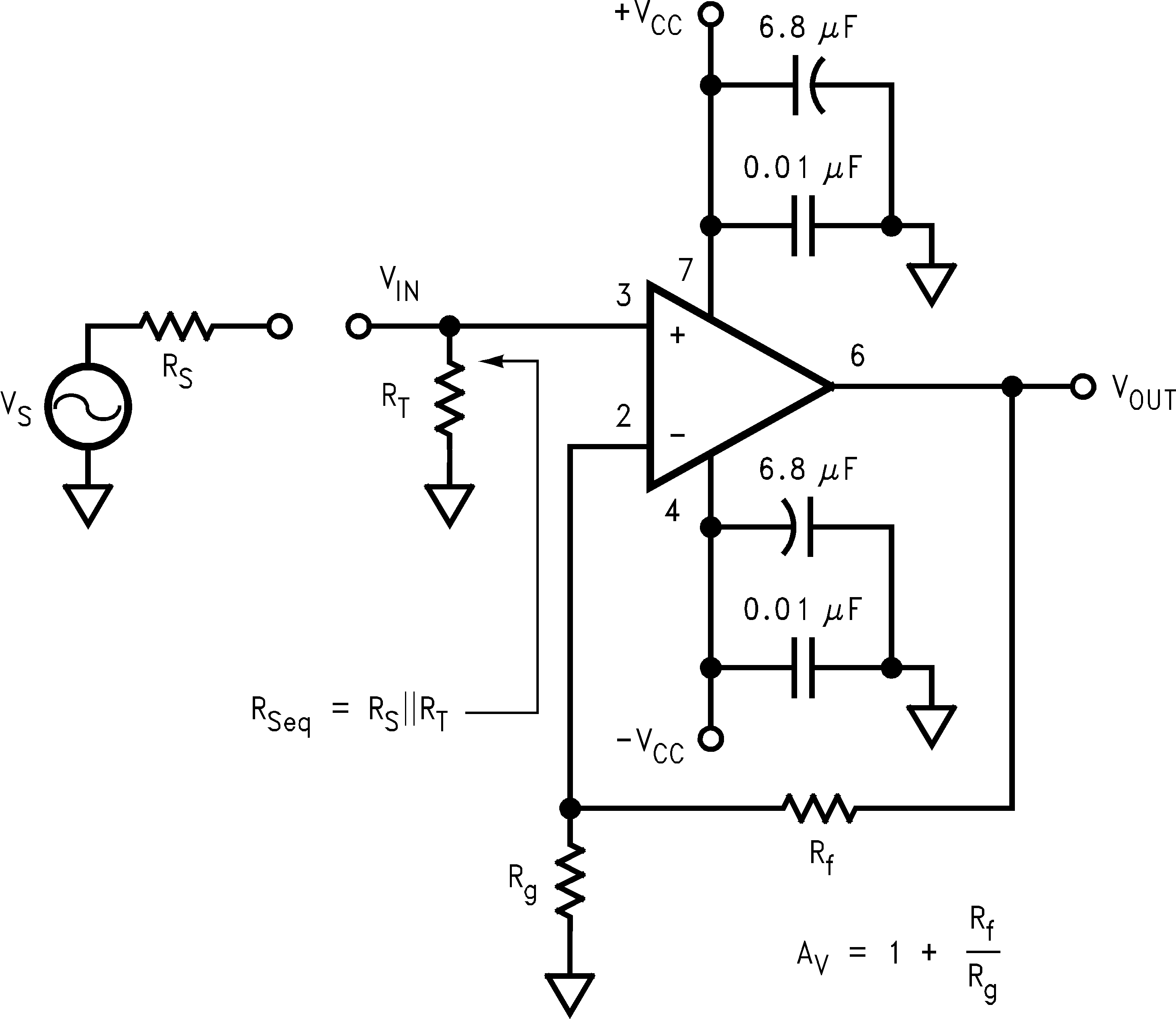 Figure 47. Non-Inverting Amplifier Configuration
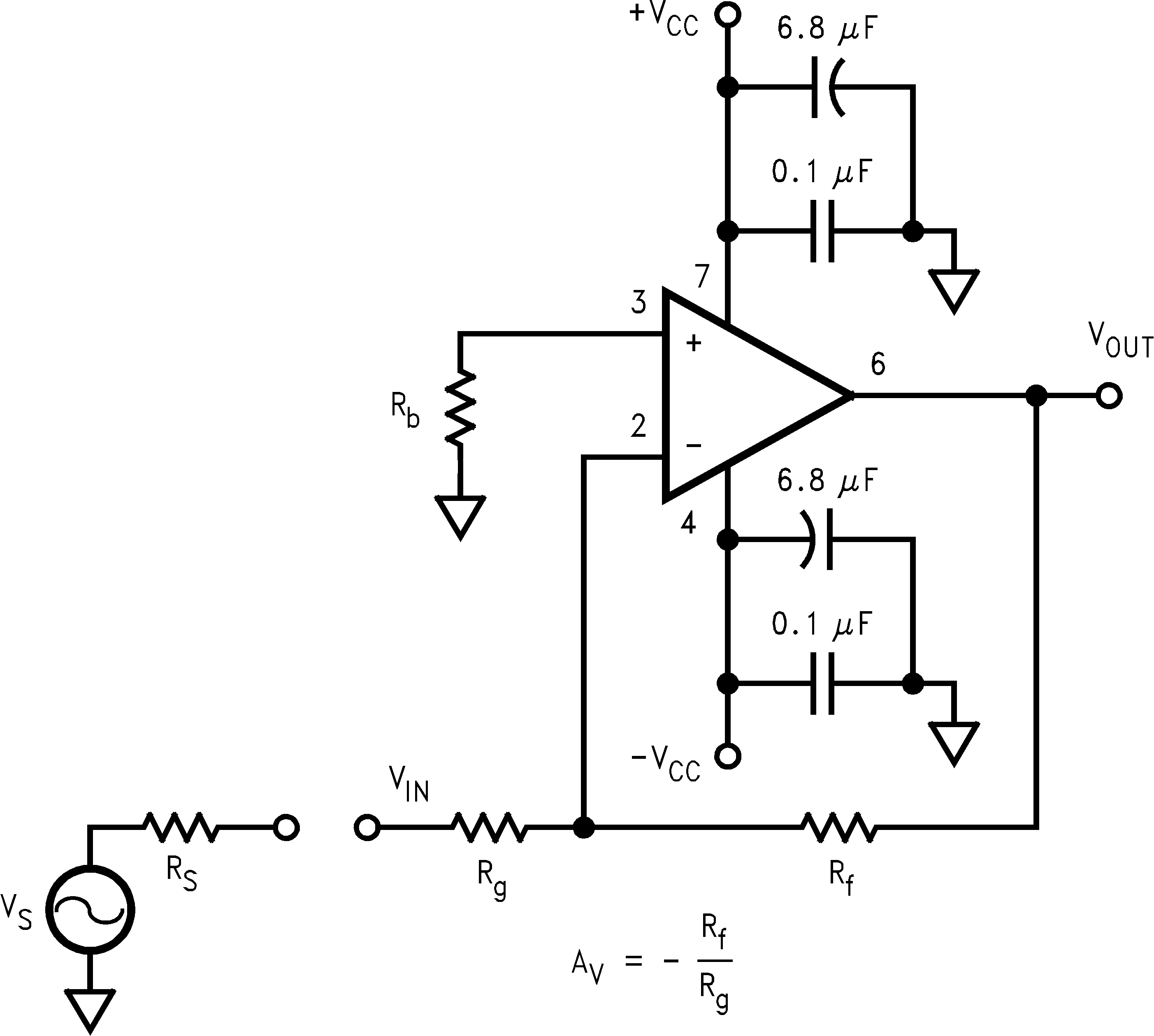 Figure 48. Inverting Amplifier Configuration
7.2.2 Total Input Noise vs. Source Resistance
To determine maximum signal-to-noise ratios from the LMH6624 and LMH6626, an understanding of the interaction between the amplifier’s intrinsic noise sources and the noise arising from its external resistors is necessary.
Figure 49 describes the noise model for the non-inverting amplifier configuration showing all noise sources. In addition to the intrinsic input voltage noise (en) and current noise (in = in+ = in−) source, there is also thermal voltage noise (et = √(4KTR)) associated with each of the external resistors. Equation 3 provides the general form for total equivalent input voltage noise density (eni). Equation 4 is a simplification of Equation 3 that assumes Rf||Rg = Rseq for bias current cancellation. Figure 50 illustrates the equivalent noise model using this assumption. Figure 51 is a plot of eni against equivalent source resistance (Rseq) with all of the contributing voltage noise sources of Equation 4. This plot gives the expected eni for a given (Rseq) which assumes Rf||Rg = Rseq for bias current cancellation. The total equivalent output voltage noise (eno) is eni*AV.
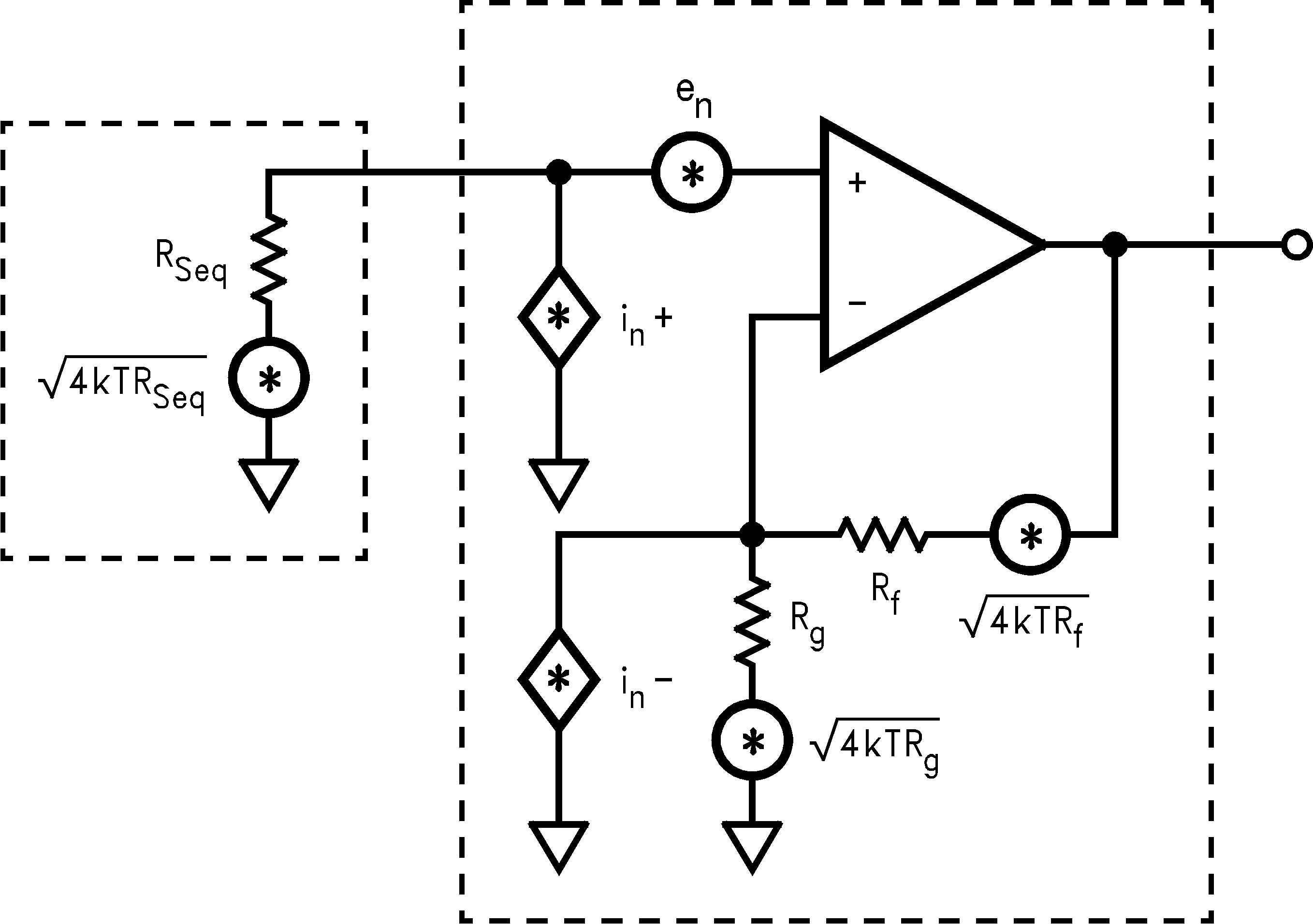 Figure 49. Non-Inverting Amplifier Noise Model

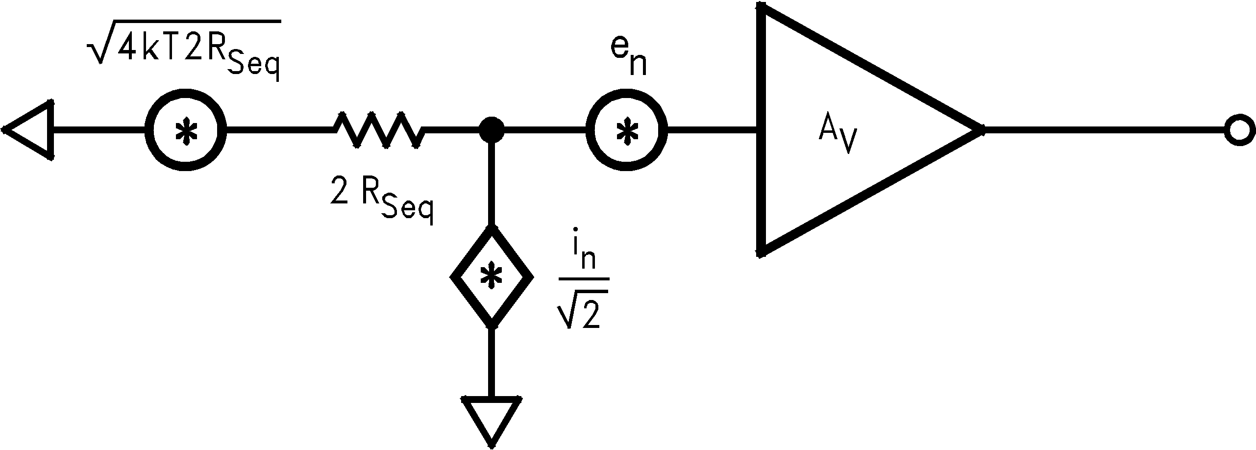 Figure 50. Noise Model with Rf||Rg = Rseq
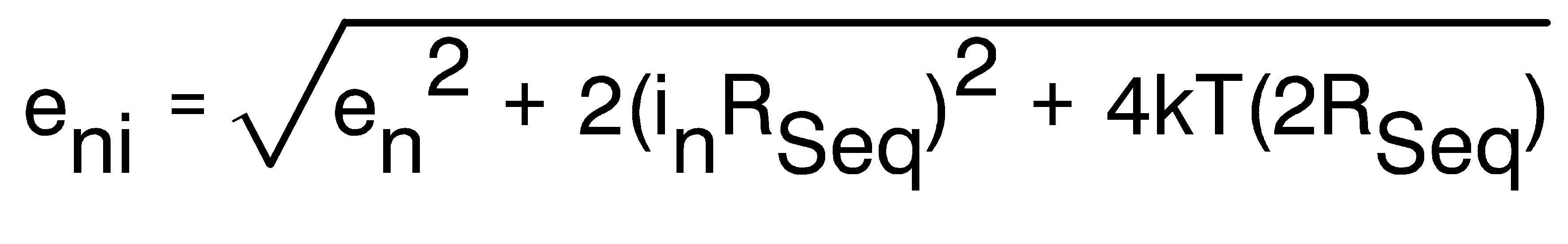
As seen in Figure 51, eni is dominated by the intrinsic voltage noise (en) of the amplifier for equivalent source resistances below 26 Ω. Between 26 Ω and 3.1 kΩ, eni is dominated by the thermal noise (et = √(4kT(2Rseq)) of the equivalent source resistance Rseq. Above 3.1 kΩ, eni is dominated by the amplifier’s current noise (in = √2 inRseq). When Rseq = 283 Ω (that is, Rseq = en/√2 in) the contribution from voltage noise and current noise of LMH6624 and LMH6626 is equal. For example, configured with a gain of +20V/V giving a −3 dB of 90 MHz and driven from Rseq = Rf || Rg = 25 Ω (eni = 1.3 nV√Hz from Figure 51), the LMH6624 produces a total output noise voltage (eni × 20 V/V × √(1.57 × 90 MHz)) of 309 μVrms.
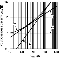 Figure 51. Voltage Noise Density vs. Source Resistance
If bias current cancellation is not a requirement, then Rf || Rg need not equal Rseq. In this case, according to Equation 3, Rf || Rg should be as low as possible to minimize noise. Results similar to Equation 3 are obtained for the inverting configuration of Figure 48 if Rseq is replaced by Rb and Rg is replaced by Rg + Rs. With these substitutions, Equation 3 will yield an eni referred to the non-inverting input. Referring eni to the inverting input is easily accomplished by multiplying eni by the ratio of non-inverting to inverting gains.
7.2.3 Noise Figure
Noise Figure (NF) is a measure of the noise degradation caused by an amplifier.
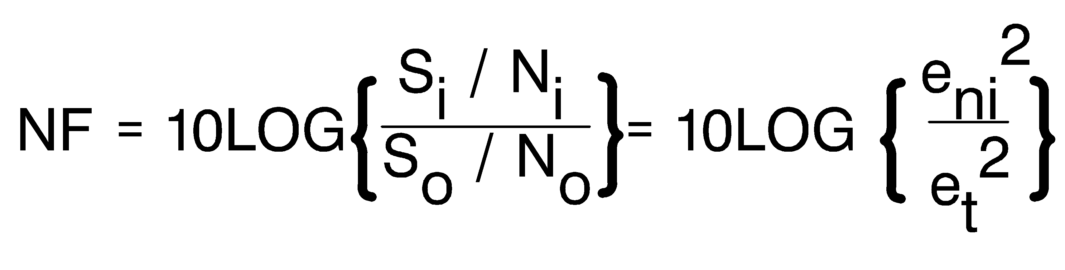
The Noise Figure formula is shown in Equation 5. The addition of a terminating resistor RT, reduces the external thermal noise but increases the resulting NF. The NF is increased because RT reduces the input signal amplitude thus reducing the input SNR.
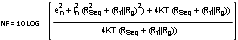
The noise figure is related to the equivalent source resistance (Rseq) and the parallel combination of Rf and Rg. To minimize "Noise Figure":
- Minimize Rf || Rg
- Choose the Optimum RS (ROPT)
ROPT is the point at which the NF curve reaches a minimum and is approximated by:

7.2.4 Low Noise Integrator
The LMH6624 and LMH6626 devices implement a deBoo integrator shown in Figure 52. Positive feedback maintains integration linearity. The low input offset voltage of the LMH6624 and LMH6626 devices and matched inputs allow bias current cancellation and provide for very precise integration. Keeping RG and RS low helps maintain dynamic stability.
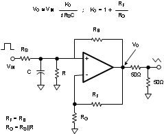 Figure 52. Low Noise Integrator
7.2.5 High-gain Sallen-key Active Filters
The LMH6624 and LMH6626 devices are well suited for high gain Sallen-Key type of active filters. Figure 53 shows the 2nd order Sallen-Key low pass filter topology. Using component predistortion methods discussed in Application Note OA-21, Component Pre-Distortion for Sallen Key Filters (SNOA369) will enable the proper selection of components for these high-frequency filters.
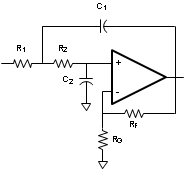 Figure 53. Sallen-Key Active Filter Topology
7.2.6 Low Noise Magnetic Media Equalizer
The LMH6624 and LMH6626 devices implement a high-performance low noise equalizer for such application as magnetic tape channels as shown in Figure 54. The circuit combines an integrator with a bandpass filter to produce the low noise equalization. The circuit’s simulated frequency response is illustrated in Figure 55.
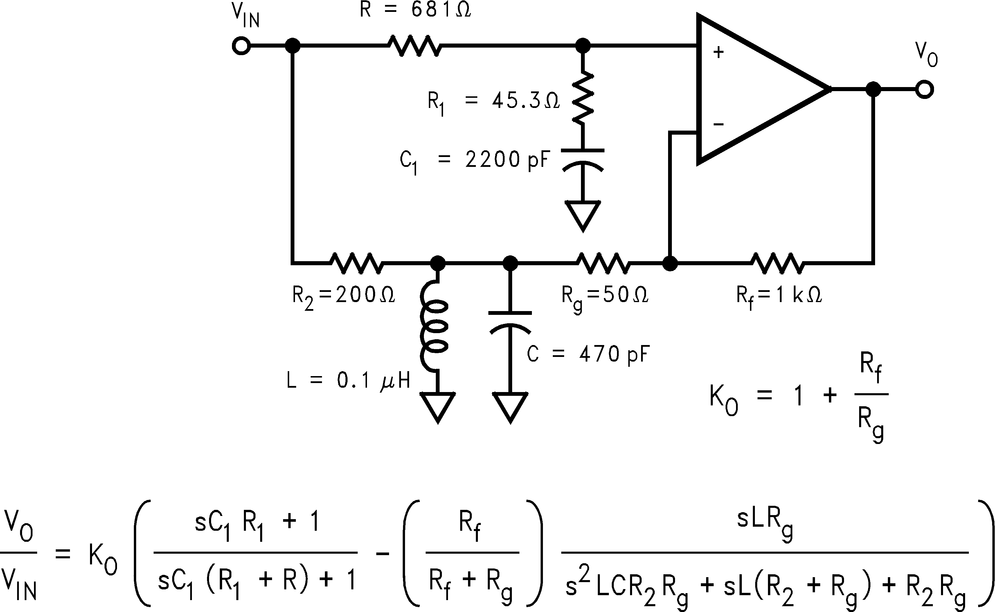 Figure 54. Low Noise Magnetic Media Equalizer
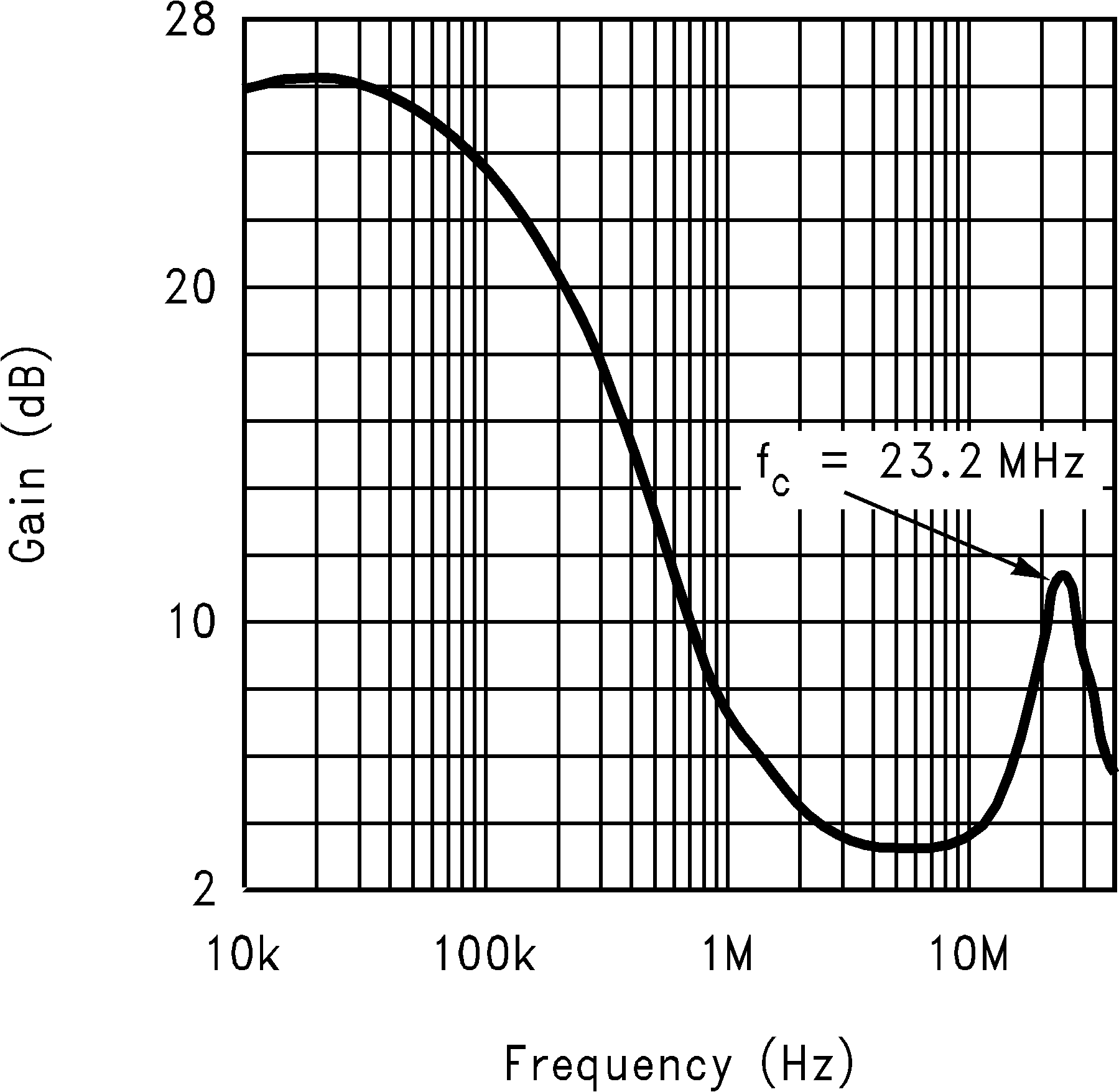 Figure 55. Equalizer Frequency Response
7.3 Device Functional Modes
7.3.1 Single Supply Operation
The LMH6624 and LMH6626 devices can be operated with single power supply as shown in Figure 56. Both the input and output are capacitively coupled to set the DC operating point.
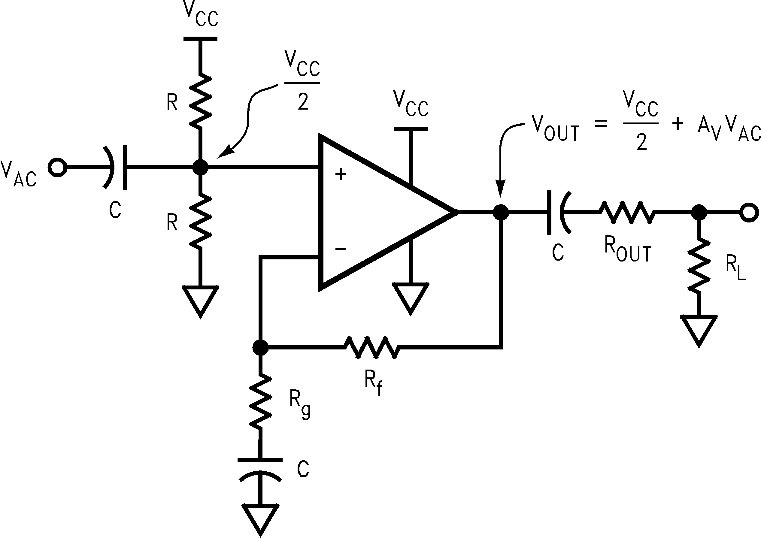 Figure 56. Single Supply Operation