SNOSAK9F June 2006 – June 2015 LMH6601 , LMH6601-Q1
PRODUCTION DATA.
- 1 Features
- 2 Applications
- 3 Description
- 4 Revision History
- 5 Pin Configuration and Functions
-
6 Specifications
- 6.1 Absolute Maximum Ratings
- 6.2 ESD Ratings - for LMH6601
- 6.3 ESD Ratings - for LMH6601-Q1
- 6.4 Recommended Operating Conditions
- 6.5 Thermal Information
- 6.6 Electrical Characteristics, 5 V
- 6.7 Electrical Characteristics, 3.3 V
- 6.8 Electrical Characteristics, 2.7 V
- 6.9 Switching Characteristics, 5 V
- 6.10 Switching Characteristics, 3.3 V
- 6.11 Switching Characteristics, 2.7 V
- 6.12 Typical Characteristics
- 7 Detailed Description
- 8 Application and Implementation
- 9 Power Supply Recommendations
- 10Layout
- 11Device and Documentation Support
- 12Mechanical, Packaging, and Orderable Information
7 Detailed Description
7.1 Overview
The high-speed, ultra-high input impedance of the LMH6601 and its fast slew rate make the device an ideal choice for video amplifier and buffering applications. There are cost benefits in having a single operating supply. Single-supply video systems can take advantage of the low supply voltage operation of the LMH6601 along with its ability to operate with input common-mode voltages at or slightly below the V− rail. Additional cost savings can be achieved by eliminating or reducing the value of the input and output AC-coupling capacitors commonly employed in single-supply video applications.
7.2 Feature Description
7.2.1 Shutdown Capability and Turn On/Off Behavior
With the device in shutdown mode, the output goes into high-impedance (ROUT > 100 MΩ) mode. In this mode, the only path between the inputs and the output pin is through the external components around the device. So, for applications where there is active signal connection to the inverting input, with the LMH6601 in shutdown, the output could show signal swings due to current flow through these external components. For noninverting amplifiers in shutdown, no output swings would occur, because of complete input-output isolation, with the exception of capacitive coupling.
For maximum power saving, the LMH6601 supply current drops to around 0.1 μA in shutdown. All significant power consumption within the device is disabled for this purpose. Because of this, the LMH6601 turnon time is measured in microseconds whereas its turnoff is fast (nanoseconds) as would be expected from a high speed device like this.
The LMH6601 SD pin is a CMOS compatible input with a pico-ampere range input current drive requirement. This pin must be tied to a level or otherwise the device state would be indeterminate. The device shutdown threshold is half way between the V+ and V− pin potentials at any supply voltage. For example, with V+ tied to 10 V and V− equal to 5 V, you can expect the threshold to be at 7.5 V. The state of the device (shutdown or normal operation) is ensured over temperature as long as the SD pin is held to within 10% of the total supply voltage.
For V+ = 10 V, V− = 5 V, as an example:
- Shutdown Range 5 V ≤ SD ≤ 5.5 V
- Normal Operation Range 9.5 V ≤ SD ≤ 10 V
7.2.2 Overload Recovery and Swing Close to Rails
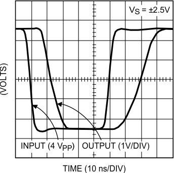
The LMH6601 can recover from an output overload in less than 20 ns. See Figure 47 for the input and output scope photos:
 Figure 47. LMH6601 Output Overload Recovery Waveform
In Figure 47, the input step function is set so that the output is driven to one rail and then the other and then the output recovery is measured from the time the input crosses 0 V to when the output reaches this point.
Also, when the LMH6601 input voltage range is exceeded near the V+ rail, the output does not experience output phase reversal, as do some op amps. This is particularly advantageous in applications where output phase reversal must be avoided at all costs, such as in servo loop control among others. This adds to the set of features of the LMH6601, which make this device easy to use.
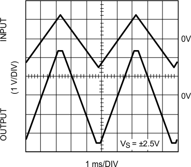
In addition, the LMH6601 output swing close to either rail is well-behaved as shown in the scope photo of Figure 48.
 Figure 48. Clean Swing of the LMH6601 to Either Rail
With some op amps, when the output approaches either one or both rails and saturation starts to set in, there is significant increase in the transistor parasitic capacitances which leads to loss of Phase Margin. That is why with these devices, there are sometimes hints of instability with output close to the rails. With the LMH6601, as can be seen in Figure 48, the output waveform remains free of instability throughout its range of voltages.
7.3 Device Functional Modes
7.3.1 Optimizing Performance
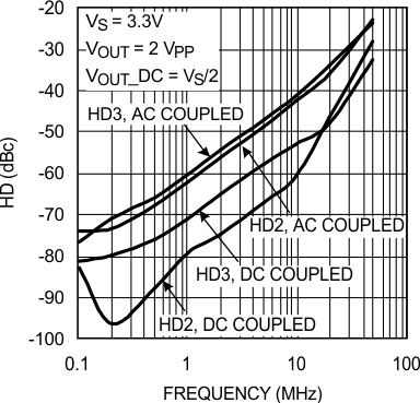
With many op amps, additional device nonlinearity and sometimes less loop stability arises when the output must switch from current-source mode to current-sink mode or vice versa. When it comes to achieving the lowest distortion and the best Differential Gain/ Differential Phase (DG/ DP, broadcast video specs), the LMH6601 is optimized for single-supply DC-coupled output applications where the load current is returned to the negative rail (V−). That is where the output stage is most linear (lowest distortion) and which corresponds to unipolar current flowing out of this device. To that effect, it is easy to see that the distortion specifications improve when the output is only sourcing current which is the distortion-optimized mode of operation for the LMH6601. In an application where the LMH6601 output is AC-coupled or when it is powered by separate dual supplies for V+ and V−, the output stage supplies both source and sink current to the load and results in less than optimum distortion (and DG/DP). Figure 49 compares the distortion results between a DC- and an AC-coupled load to show the magnitude of this difference. See the DG/DP plots, Figure 43 through Figure 46, in Typical Characteristics, for a comparison between DC- and AC-coupling of the video load.
 Figure 49. Distortion Comparison between DC- and AC-Coupling of the Load
In certain applications, it may be possible to optimize the LMH6601 for best distortion (and DG/DP) even though the load may require bipolar output current by adding a pulldown resistor to the output. Adding an output pulldown resistance of appropriate value could change the LMH6601 output loading into source-only. This comes at the price of higher total power dissipation and increased output current requirement.
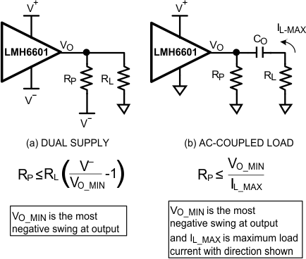
Figure 50 shows how to calculate the pulldown resistor value for both the dual-supply and for the AC-coupled load applications.
 Figure 50. Output Pulldown Value for Dual-Supply and AC-Coupling
Furthermore, with a combination of low closed-loop gain setting (that is, AV = +1 for example where device bandwidth is the highest), light output loading (RL > 1 kΩ) , and with a significant capacitive load (CL > 10 pF) , the LMH6601 is most stable if output sink current is kept to less than about 5 mA. The pulldown method described in Figure 50 is applicable in these cases as well where the current that would normally be sunk by the op amp is diverted to the RP path instead.