SNAS393D March 2007 – November 2016 LME49720
PRODUCTION DATA.
- 1 Features
- 2 Applications
- 3 Description
- 4 Revision History
- 5 Device Comparison Table
- 6 Pin Configuration and Functions
- 7 Specifications
- 8 Parameter Measurement Information
- 9 Detailed Description
- 10Application and Implementation
- 11Power Supply Recommendations
- 12Layout
- 13Device and Documentation Support
- 14Mechanical, Packaging, and Orderable Information
10 Application and Implementation
NOTE
Information in the following applications sections is not part of the TI component specification, and TI does not warrant its accuracy or completeness. TI’s customers are responsible for determining suitability of components for their purposes. Customers should validate and test their design implementation to confirm system functionality.
10.1 Application Information
These typical connection diagrams highlight the required external components and system level connections for proper operation of the device. Any design variation can be supported by TI through schematic and layout reviews. Visit e2e.ti.com for design assistance and join the audio amplifier discussion forum for additional information
10.2 Typical Applications
10.2.1 Single Ended Converter
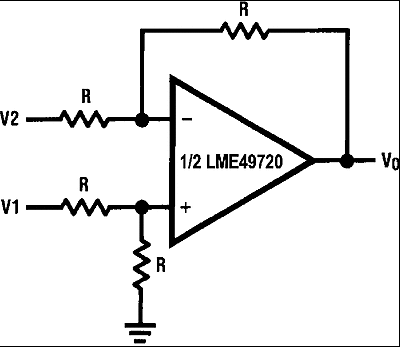
10.2.1.1 Design Requirements
For this design example, use the parameters listed in Table 1.
Table 1. Design Parameters
| DESIGN PARAMETER | EXAMPLE VALUE |
|---|---|
| Power Supply | ±15 |
| Speaker | 2 KΩ |
10.2.1.2 Detailed Design Procedure
10.2.1.2.1 Surface Mount Capacitors
Temperature and applied DC voltage influence the actual capacitance of high-K materials. Table 2 shows the relationship between the different types of high-K materials and their associated tolerances, temperature coefficients, and temperature ranges. Notice that a capacitor made with X5R material can lose up to 15% of its capacitance within its working temperature range.
Select high-K ceramic capacitors according to the following rules:
- Use capacitors made of materials with temperature coefficients of X5R, X7R, or better.
- Use capacitors with DC voltage ratings of at least twice the application voltage.
- Choose a capacitance value at least twice the nominal value calculated for the application.
Multiply the nominal value by a factor of 2 for safety. If a 10-µF capacitor is required, use 20µF.
The preceding rules and recommendations apply to capacitors used in connection with this device. The LME49720 cannot meet its performance specifications if the rules and recommendations are not followed.
Table 2. Typical Tolerance and Temperature Coefficient of Capacitance by Material
| Material | COG/NPO | X7R | X5R |
|---|---|---|---|
| Typical Tolerance | ±5% | ±10% | 80/–20% |
| Temperature | ±30ppm | ±15% | 22/–82% |
| Temperature Range, ºC | –55/125ºC | –55/125ºC | –30/85 ºC |
10.2.2 Other Applications
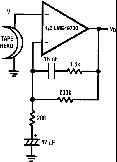
F = 1 kHz
En = 0.38 μV
A Weighted
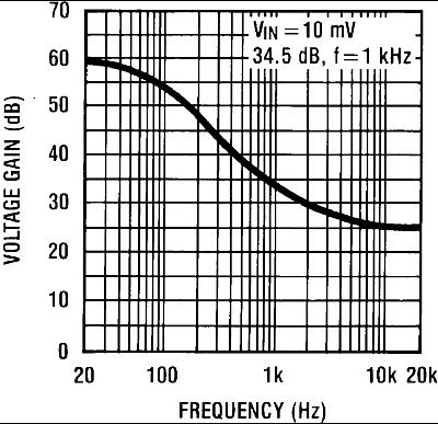
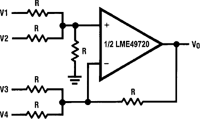
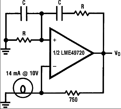

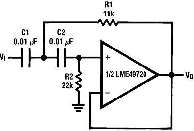
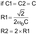
Illustration is f0 = 1 kHz
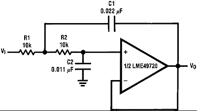
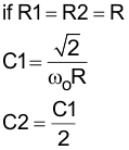
Illustration is f0 = 1 kHz
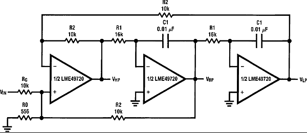

Illustration is f0 = 1 kHz, Q = 10, ABP = 1
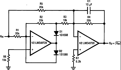
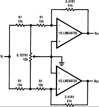
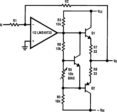
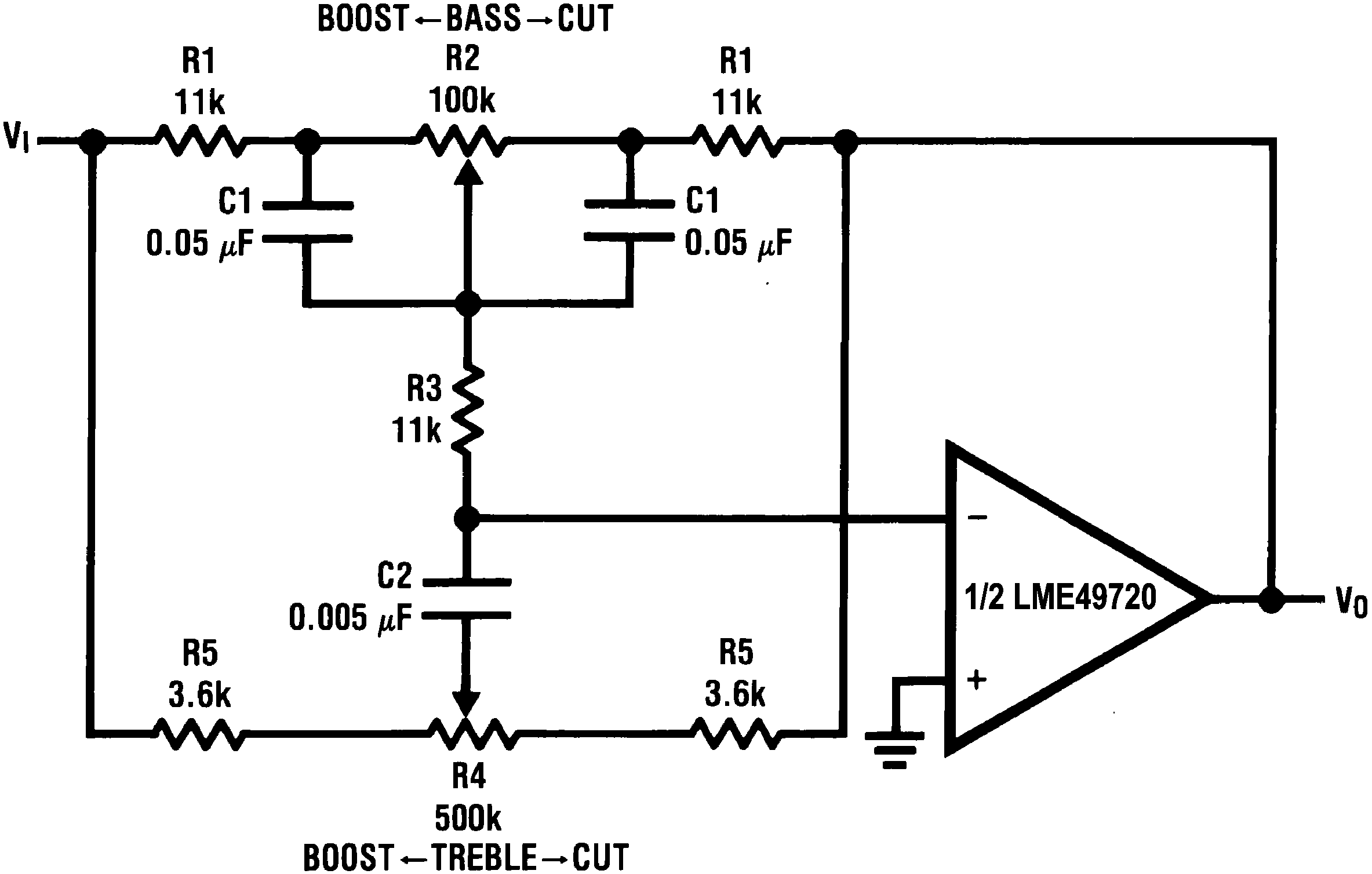

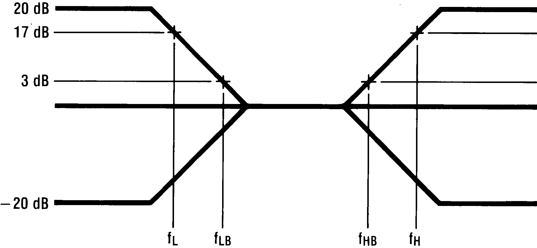
Illustration is:
fL = 32 Hz, fLB = 320 Hz
fH =11 kHz, fHB = 1.1 kHz
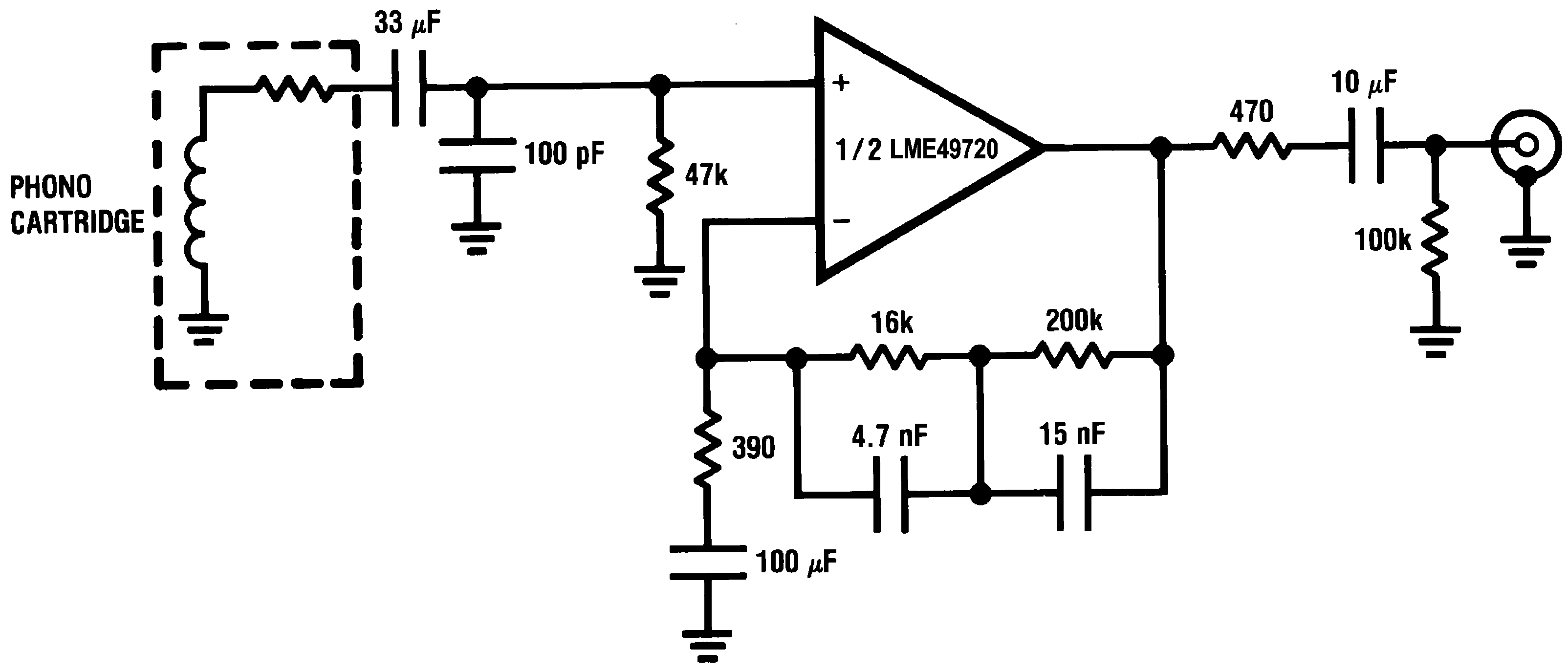
En = 0.33 μV
S/N = 90 dB
f = 1 kHz
A Weighted
A Weighted, VIN = 10 mV
@f = 1 kHz
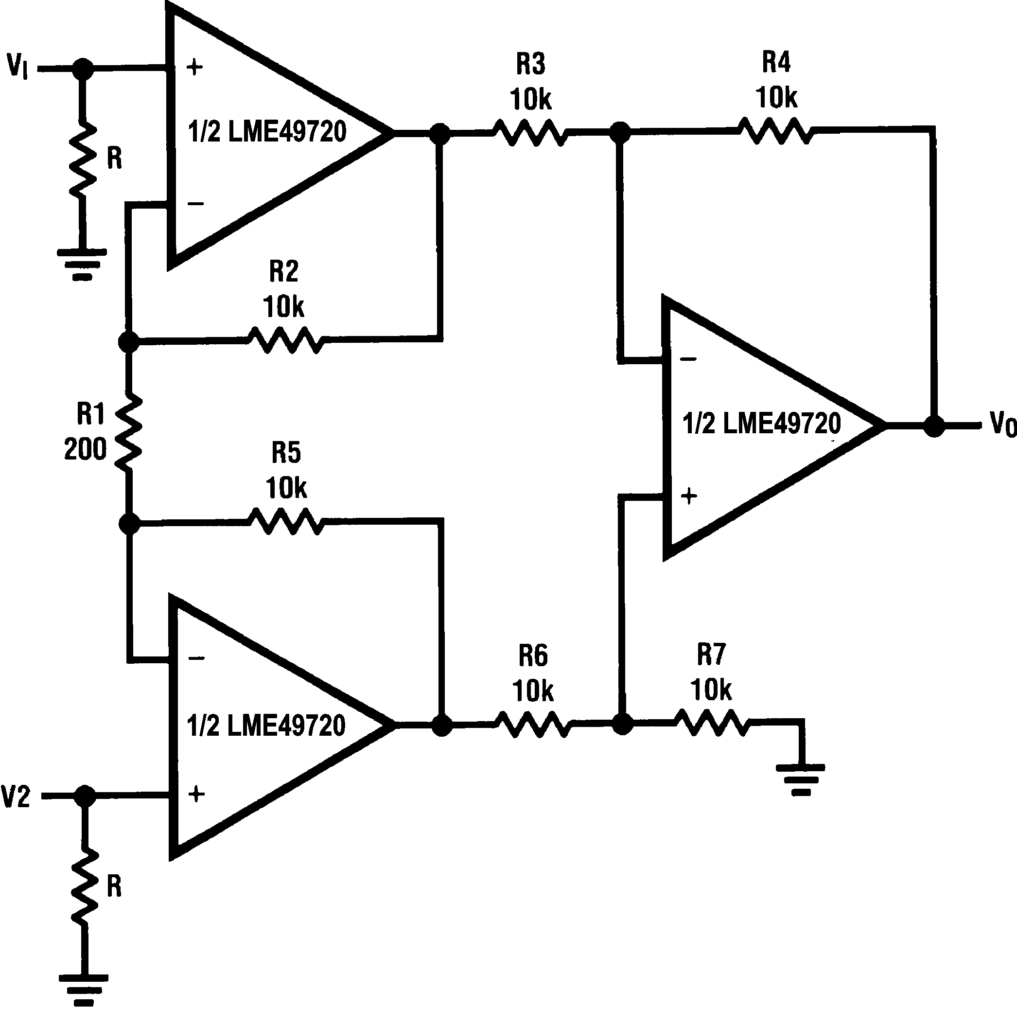

Illustration is:
V0 = 101(V2 − V1)
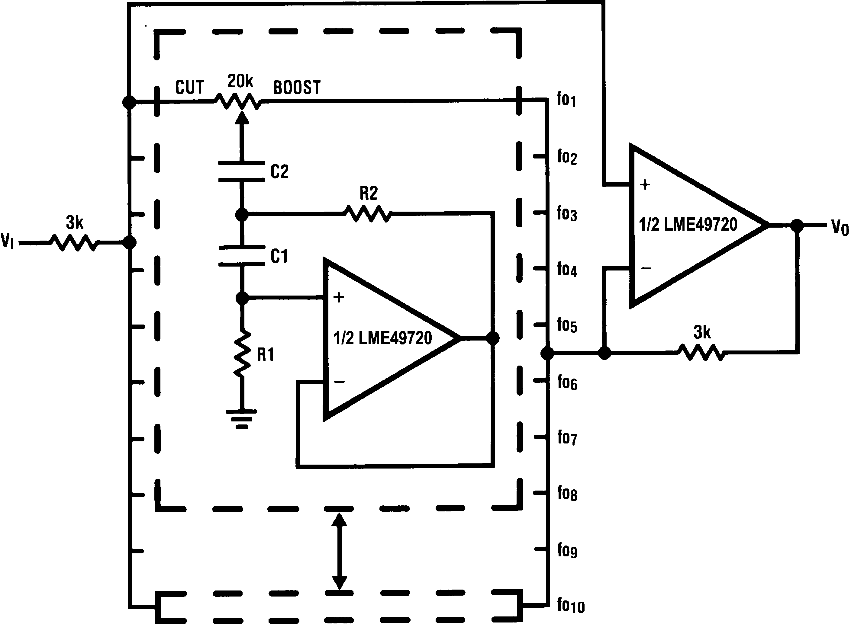
Table 4. Typical Values for Band Graphic Equalizer
| fo (Hz) | C1 | C2 | R1 | R2 |
|---|---|---|---|---|
| 32 | 0.12μF | 4.7μF | 75kΩ | 500Ω |
| 64 | 0.056μF | 3.3μF | 68kΩ | 510Ω |
| 125 | 0.033μF | 1.5μF | 62kΩ | 510Ω |
| 250 | 0.015μF | 0.82μF | 68kΩ | 470Ω |
| 500 | 8200pF | 0.39μF | 62kΩ | 470Ω |
| 1k | 3900pF | 0.22μF | 68kΩ | 470Ω |
| 2k | 2000pF | 0.1μF | 68kΩ | 470Ω |
| 4k | 1100pF | 0.056μF | 62kΩ | 470Ω |
| 8k | 510pF | 0.022μF | 68kΩ | 510Ω |
| 16k | 330pF | 0.012μF | 51kΩ | 510Ω |