SNOSBY1C June 1999 – December 2015 LMC567
PRODUCTION DATA.
- 1 Features
- 2 Applications
- 3 Description
- 4 Revision History
- 5 Device Comparison Table
- 6 Pin Configuration and Functions
- 7 Specifications
- 8 Parameter Measurement Information
- 9 Detailed Description
- 10Application and Implementation
- 11Power Supply Recommendations
- 12Layout
- 13Device and Documentation Support
- 14Mechanical, Packaging, and Orderable Information
9 Detailed Description
9.1 Overview
The LMC567C is a low-power, general-purpose tone decoder with similar functionality to the industry standard LM567. The device requires external components set up the internal oscillator to run at twice the input frequency and determine the required filter constants. Internal VCO and Phase detector form a Phase-locked loop which locks to an input signal frequency that is established by external timing components. When PLL is locked, a switch to ground is activated in the output of the device.
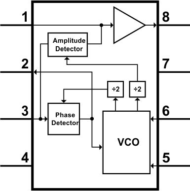
9.2 Functional Block Diagram

9.3 Feature Description
9.3.1 Oscillator
The voltage-controlled oscillator (VCO) on the LMC567 must be set up to run at twice the frequency of the input signal tone to be decoded. The center frequency of the VCO is set by timing resistor Rt and timing capacitor Ct connected to pins 5 and 6 of the IC. The center frequency as a function of Rt and Ct is given by Equation 4:

Because this causes an input tone of half Fosc to be decoded by Equation 5,

Equation 5 is accurate at low frequencies; however, above 50 kHz (Fosc = 100 kHz), internal delays cause the actual frequency to be lower than predicted.
The choice of Rt and Ct is a tradeoff between supply current and practical capacitor values. An additional supply current component is introduced in Equation 6 due to Rt being switched to Vs every half cycle to charge Ct:
Thus the supply current can be minimized by keeping Rt as large as possible (see Figure 1). However, the desired frequency dictates an RtCt product such that increasing Rt requires a smaller Ct. Below
Ct = 100 pF, circuit board stray capacitances begin to play a role in determining the oscillation frequency which ultimately limits the minimum Ct.
To allow for IC and component value tolerances, the oscillator timing components requires a trim. This is generally accomplished by using a variable resistor as part of Rt, although Ct could also be padded. The amount of initial frequency variation due to the LMC567 itself is given in the Electrical Characteristics; the total trim range must also accommodate the tolerances of Rt and Ct.
9.3.2 Input
The input pin 3 is internally ground-referenced with a nominal 40-kΩ resistor. Signals which are already centered on 0 V may be directly coupled to pin 3; however, any DC potential must be isolated through a coupling capacitor. Inputs of multiple LMC567 devices can be paralleled without individual DC isolation.
9.3.3 Loop Filter
Pin 2 is the combined output of the phase detector and control input of the VCO for the phase-locked loop (PLL). Capacitor C2 in conjunction with the nominal 80-kΩ pin 2 internal resistance forms the loop filter.
For small values of C2, the PLL has a fast acquisition time and the pull-in range is set by the built in VCO frequency stops, which also determines the largest detection bandwidth (LDBW). Increasing C2 results in improved noise immunity at the expense of acquisition time, and the pull-in range begins to become narrower than the LDBW (see Figure 4). However, the maximum hold-in range always equal the LDBW.
9.3.4 Output Filter
Pin 1 is the output of a negative-going amplitude detector which has a nominal 0 signal output of 7/9 Vs. When the PLL is locked to the input, an increase in signal level causes the detector output to move negative. When pin 1 reaches 2/3 Vs, the output is activated (see Output).
Capacitor C1 in conjunction with the nominal 40-kΩ pin 1 internal resistance forms the output filter. The size of C1 is a tradeoff between slew rate and carrier ripple at the output comparator. Low values of C1 produce the least delay between the input and output for tone burst applications, while larger values of C1 improve noise immunity.
Pin 1 also provides a means for shifting the input threshold higher or lower by connecting an external resistor to supply or ground. However, reducing the threshold using this technique increases sensitivity to pin 1 carrier ripple and also results in more part to part threshold variation.
9.3.5 Output
The output at pin 8 is an N-channel FET switch to ground which is activated when the PLL is locked and the input tone is of sufficient amplitude to cause pin 1 to fall below 2/3 Vs. Apart from the obvious current component due to the external pin 8 load resistor, no additional supply current is required to activate the switch. The ON-resistance of the switch is inversely proportional to supply; thus the sat voltage for a given output current increases at lower supplies.
9.4 Device Functional Modes
9.4.1 Operation as LM567
The LMC567 low power tone decoder can be operated at supply voltages of 2 V to 9 V and at input frequencies ranging from 1 Hz up to 500 kHz.
The LMC567 can be directly substituted in most LM567 applications with the following provisions:
- Oscillator timing capacitor Ct must be halved to double the oscillator frequency relative to the input frequency (see Oscillator).
- Filter capacitors C1 and C2 must be reduced by a factor of 8 to maintain the same filter time constants.
- The output current demanded of pin 8 must be limited to the specified capability of the LMC567.