ZHCSE83A July   2015  – October 2015 LM74610-Q1

PRODUCTION DATA.  

  1. 特性
  2. 应用
  3. 说明
  4. 修订历史记录
  5. Pin Configuration and Functions
  6. Specifications
    1. 6.1 Absolute Maximum Ratings
    2. 6.2 ESD Ratings
    3. 6.3 Recommended Operating Conditions
    4. 6.4 Thermal Information
    5. 6.5 Electrical Characteristics
    6. 6.6 Typical Characteristics
  7. Detailed Description
    1. 7.1 Overview
    2. 7.2 Functional Block Diagram
    3. 7.3 Feature Description
      1. 7.3.1 During T0
      2. 7.3.2 During T1
      3. 7.3.3 Pin Operation
        1. 7.3.3.1 Anode and Cathode Pins
        2. 7.3.3.2 VcapH and VcapL Pins
        3. 7.3.3.3 Gate Drive Pin
        4. 7.3.3.4 Gate Pull Down Pin
    4. 7.4 Device Functional Modes
      1. 7.4.1 Duty Cycle Calculation
  8. Application and Implementation
    1. 8.1 Application Information
    2. 8.2 Typical Application
      1. 8.2.1 Design Requirements
      2. 8.2.2 Detailed Design Procedure
        1. 8.2.2.1 Design Considerations
        2. 8.2.2.2 Startup Voltage
        3. 8.2.2.3 Capacitor Selection
        4. 8.2.2.4 MOSFET Selection
      3. 8.2.3 Application Curves
      4. 8.2.4 Selection of TVS Diodes in Automotive Reverse Polarity Applications
      5. 8.2.5 OR-ing Application Configuration
      6. 8.2.6 Design Requirements
  9. Power Supply Recommendations
  10. 10Layout
    1. 10.1 Layout Guidelines
    2. 10.2 Layout Example
  11. 11器件和文档支持
    1. 11.1 社区资源
    2. 11.2 商标
    3. 11.3 静电放电警告
    4. 11.4 Glossary
  12. 12机械封装和可订购信息

封装选项

机械数据 (封装 | 引脚)
散热焊盘机械数据 (封装 | 引脚)
订购信息

5 Pin Configuration and Functions

DGK Package
8-Pin VSSOP
Top View
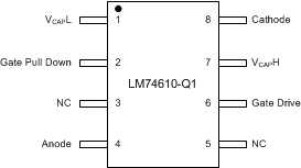
LM74610-Q1 pin_diagram_snoscz1.gif

Pin Functions

PIN NO. NAME DESCRIPTION
1 VcapL Charge Pump Output, connect to an external charge pump capacitor
2 Gate Pull Down Connect to the gate of the external MOSFET for fast turn OFF in the case of reverse polarity
3 NC No connect. Leave floating or connect to Anode pin
4 Anode Anode of the diode, connect to source of the external MOSFET
5 NC No connect. Leave floating or connect to gate drive pin
6 Gate Drive Gate Drive output, Connect to the Gate of the external MOSFET
7 VcapH Charge Pump Output, connect to an external charge pump capacitor
8 Cathode Cathode of the diode, connect to Drain of the external MOSFET