SNOS750A August 1999 – October 2014 LM7121
PRODUCTION DATA.
- 1Features
- 2Applications
- 3Description
- 4Revision History
- 5Pin Configuration and Functions
-
6Specifications
- 6.1 Absolute Maximum Ratings
- 6.2 Handling Ratings
- 6.3 Recommended Operating Conditions
- 6.4 Thermal Information
- 6.5 ±15V DC Electrical Characteristics
- 6.6 ±15V AC Electrical Characteristics
- 6.7 ±5V DC Electrical Characteristics
- 6.8 ±5V AC Electrical Characteristics
- 6.9 +5V DC Electrical Characteristics
- 6.10 +5V AC Electrical Characteristics
- 6.11 Typical Characteristics
- 7Application and Implementation
- 8Device and Documentation Support
- 9Mechanical, Packaging, and Orderable Information
7 Application and Implementation
NOTE
Information in the following applications sections is not part of the TI component specification, and TI does not warrant its accuracy or completeness. TI’s customers are responsible for determining suitability of components for their purposes. Customers should validate and test their design implementation to confirm system functionality.
7.1 Application Information
Table 1 depicts the maximum operating supply voltage for each package type
Table 1. Maximum Supply Voltage Values
| SOT-23 | SO-8 | |
|---|---|---|
| Single Supply | 10 V | 30 V |
| Dual Supplies | ±5 V | ±15 V |
Stable unity gain operation is possible with supply voltage of 5 V for all capacitive loads. This allows the possibility of using the device in portable applications with low supply voltages with minimum components around it.
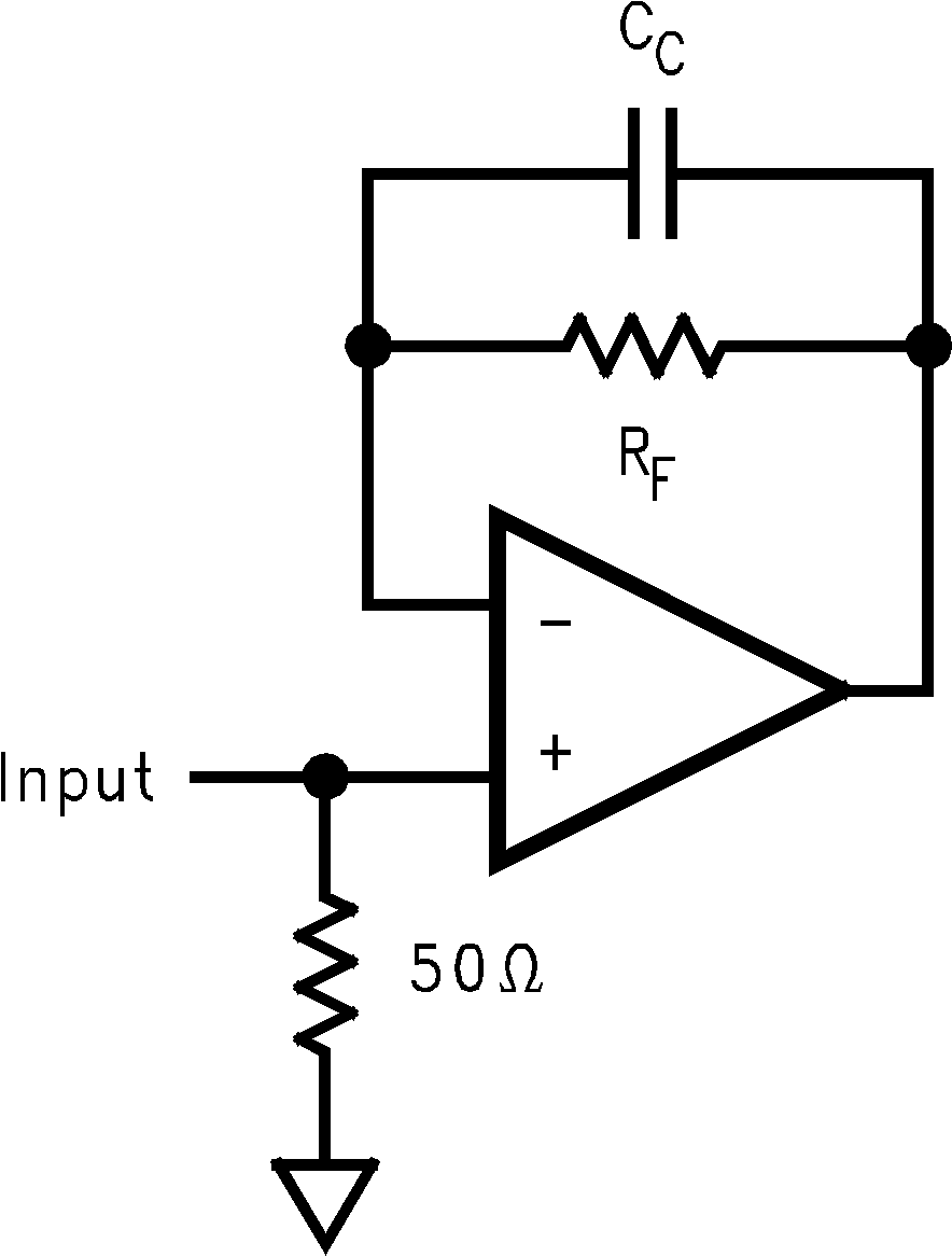
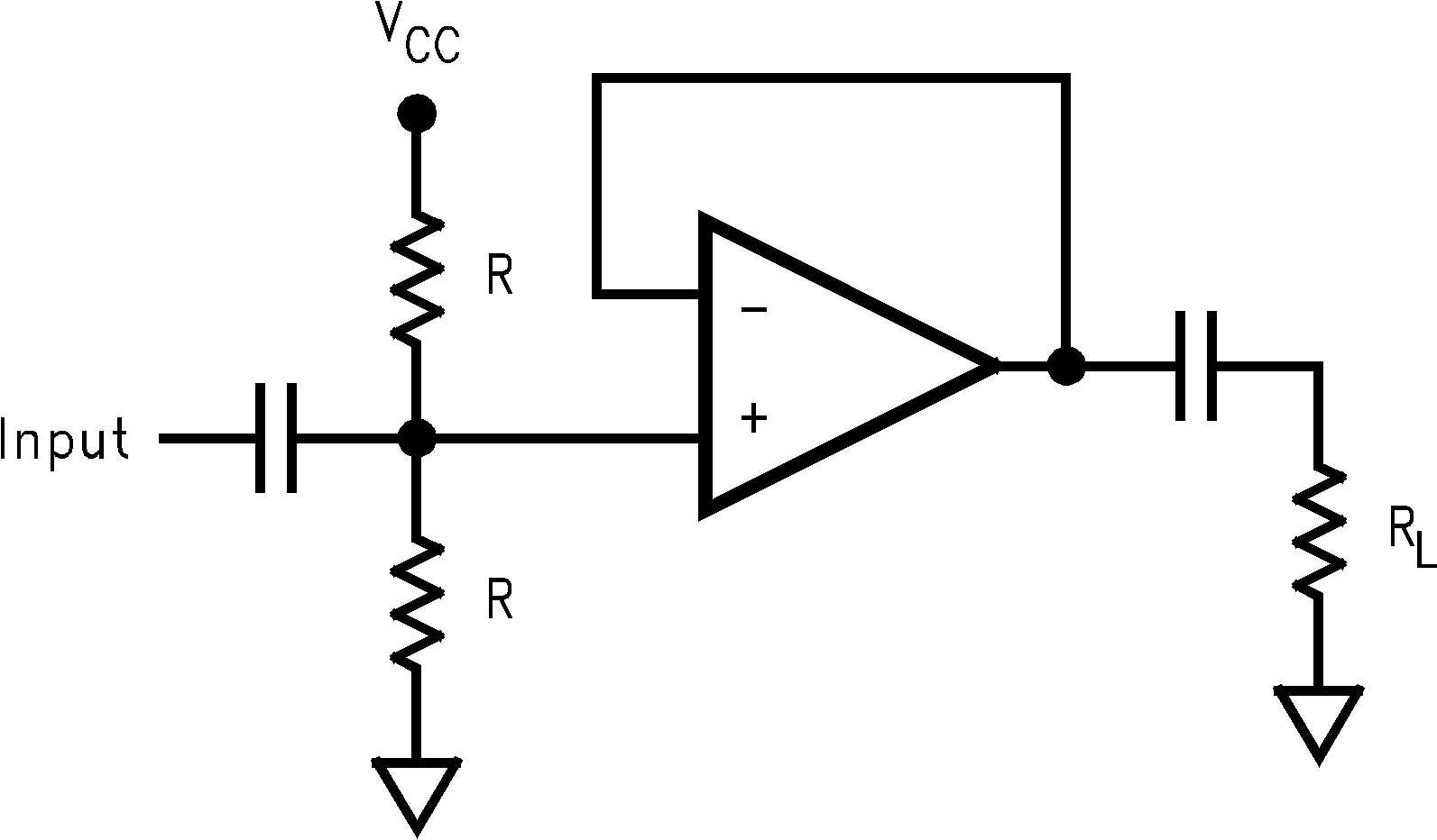
Above a supply voltage of 6 V (±3 V Dual supplies), an additional resistor and capacitor (shown in Figure 69) should be placed in the feedback path to achieve stability at unity gain over the full temperature range.
The package power dissipation should be taken into account when operating at high ambient temperatures and/or high power dissipative conditions. Refer to the power derating curves in the data sheet for each type of package.
In determining maximum operable temperature of the device, make sure the total power dissipation of the device is considered; this includes the power dissipated in the device with a load connected to the output as well as the nominal dissipation of the op amp.
The device is capable of tolerating momentary short circuits from its output to ground but prolonged operation in this mode will damage the device, if the maximum allowed junction temperation is exceeded.
7.2 Typical Applications
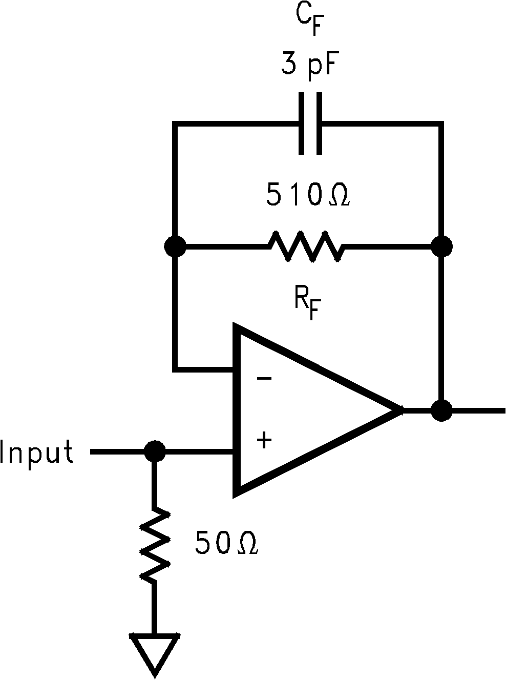 Figure 69. Typical Circuit for AV = +1 Operation (VS = 6 V)
 Figure 70. Simple Circuit to Improve Linearity and Output Drive Current
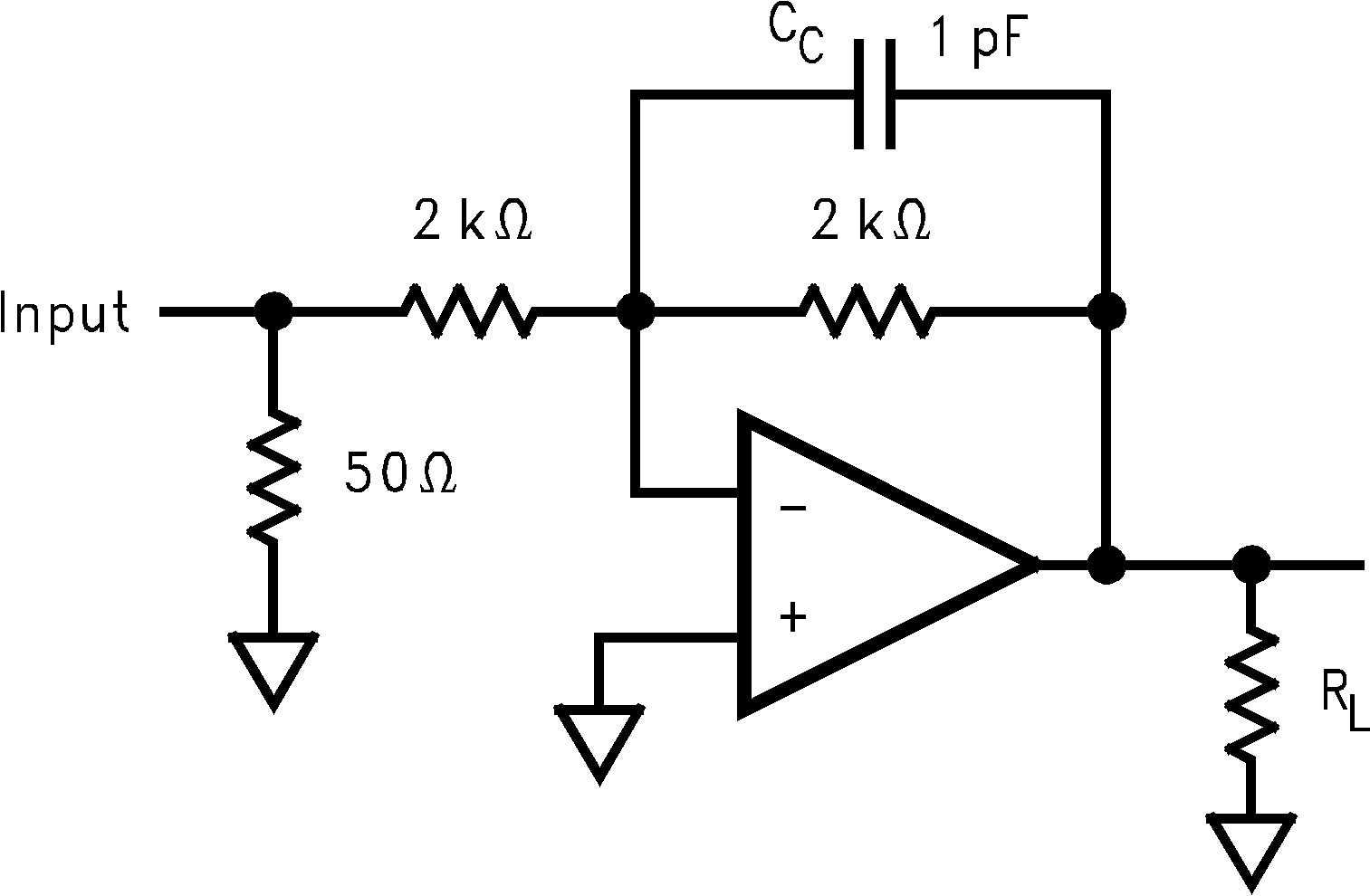 Figure 71. AV = -1
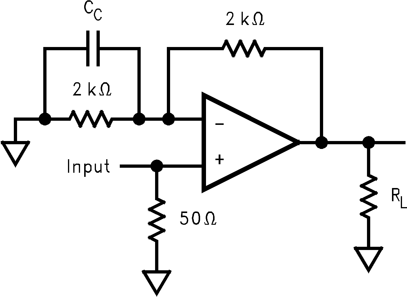
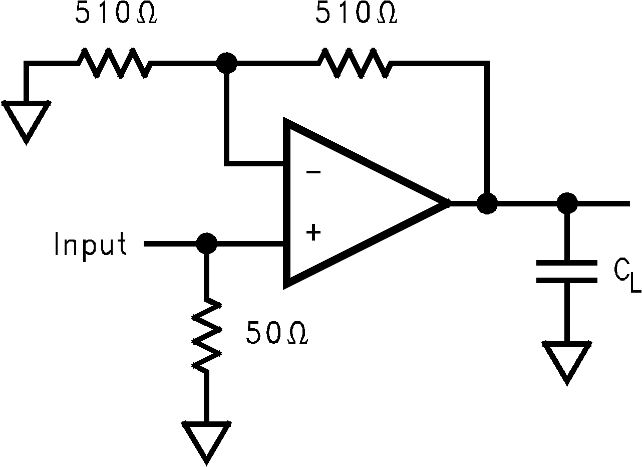 Figure 73. AV = +2, Capacitive Load
7.2.1 Design Requirements
7.2.1.1 Current Boost Circuit
The circuit in Figure 70 can be used to achieve good linearity along with high output current capability.
By proper choice of R3, the LM7121 output can be set to supply a minimal amount of current, thereby improving its output linearity.
R3 can be adjusted to allow for different loads:
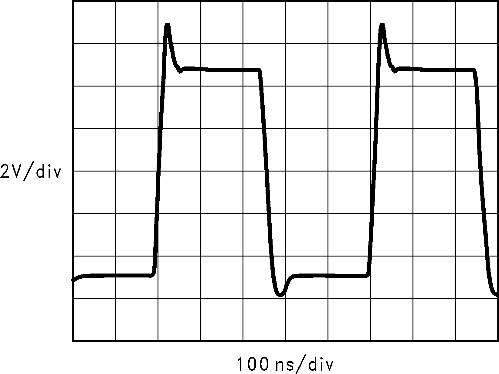
Figure 70 has been set for a load of 100 Ω. Reasonable speeds (< 30 ns rise and fall times) can be expected up to 120 mApp of load current (see Figure 77 for step response across the load).
7.2.2 Detailed Design Procedure
It is very important to keep the lead lengths to a minimum and to provide a low impedance current path by using a ground-plane on the board.
CAUTION
If RL is removed, the current balance at the output of LM7121 would be disturbed and it would have to supply the full amount of load current. This might damage the part if power dissipation limit is exceeded.
7.2.2.1 Color Video on Twisted Pairs Using Single Supply
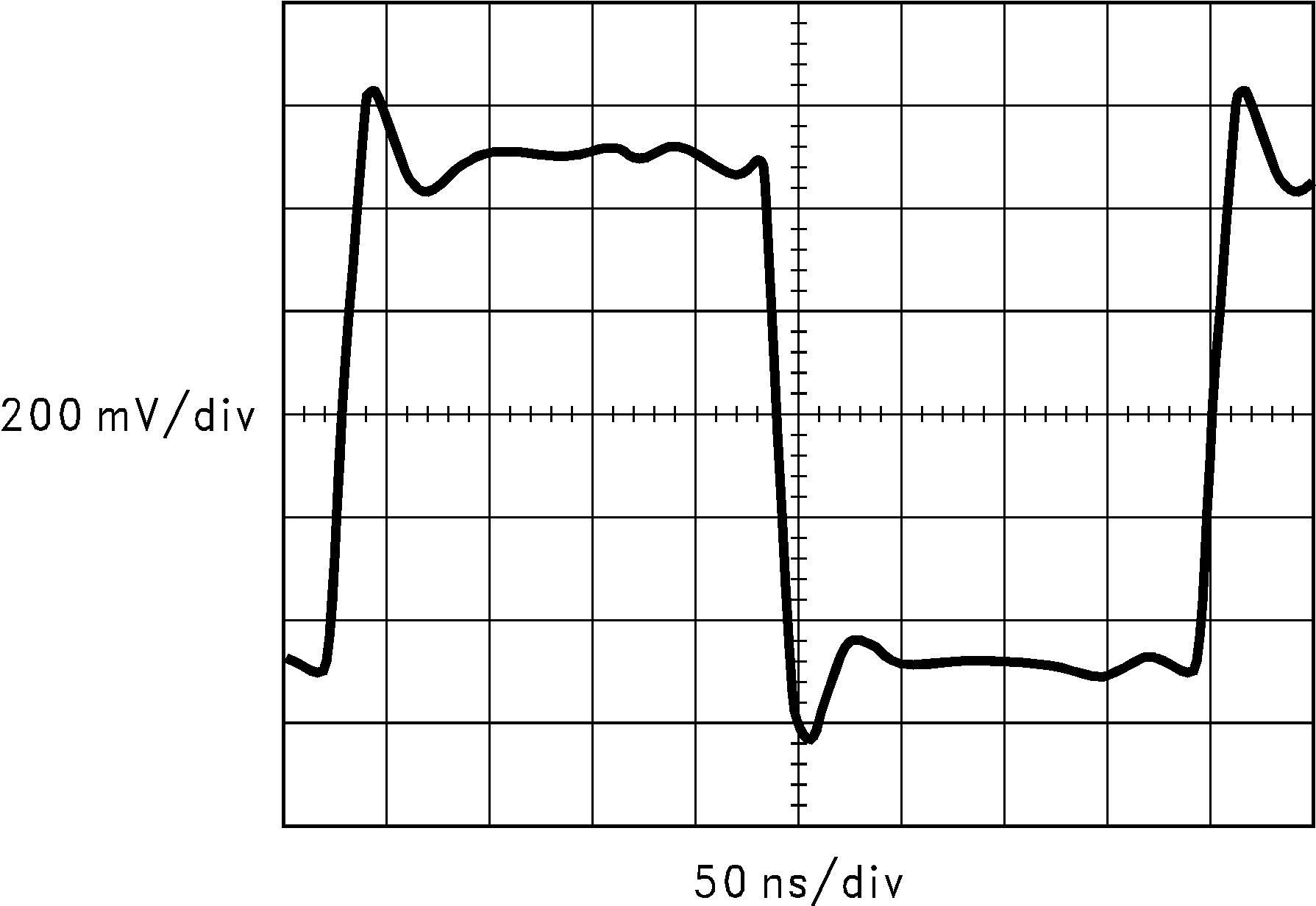
The circuit shown in Figure 76 can be used to drive in excess of 25 meters length of twisted pair cable with no loss of resolution or picture definition when driving a NTSC monitor at the load end.
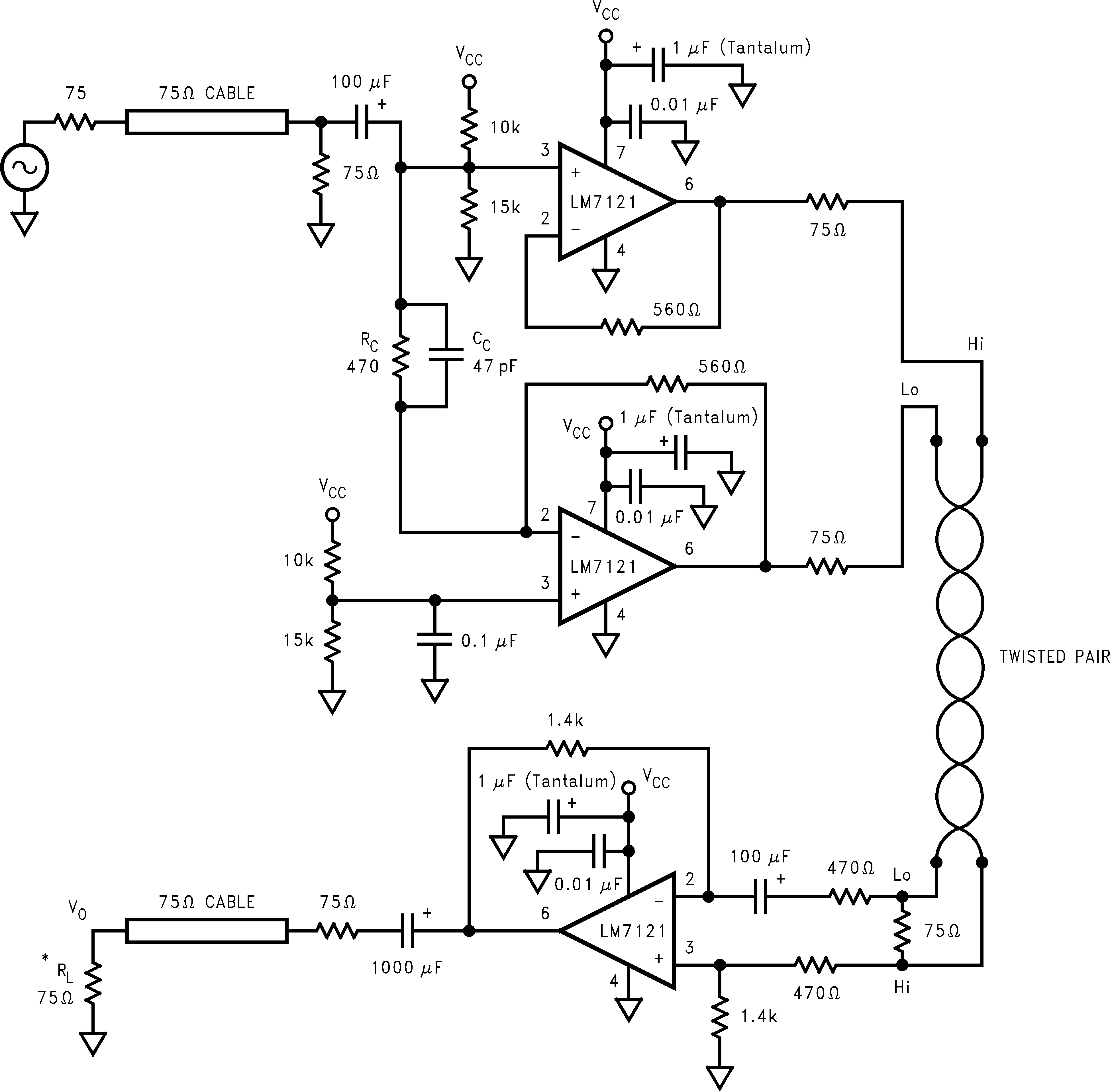
8.5 V ≤ VCC ≤ 30 V
Differential Gain and Differential Phase errors measured at the load are less than 1% and 1˚ respectively
RG and CC can be adjusted for various cable lengths to compensate for the line losses and for proper response at the output. Values shown correspond to a twisted pair cable length of 25 meters with about 3 turns/inch (see Figure 78 for step response).
The supply voltage can vary from 8.5 V up to 30 V with the output rise and fall times under 12 ns. With the component values shown, the overall gain from the input to the output is about 1.
Even though the transmission line is not terminated in its nominal characteristic impedance of about 600 Ω, the resulting reflection at the load is only about 5% of the total signal and in most cases can be neglected. Using 75 termination instead, has the advantage of operating at a low impedance and results in a higher realizable bandwidth and signal fidelity.
7.2.3 Application Performance Plots