ZHCSHU8F October   2008  – July 2019 LM5575-Q1

PRODUCTION DATA.  

  1. 特性
  2. 应用
  3. 说明
    1.     Device Images
      1.      简化原理图
  4. 修订历史记录
  5. Pin Configuration and Functions
    1.     Pin Functions
  6. Specifications
    1. 6.1 Absolute Maximum Ratings
    2. 6.2 ESD Ratings
    3. 6.3 Recommended Operating Conditions
    4. 6.4 Thermal Information
    5. 6.5 Electrical Characteristics
    6. 6.6 Typical Characteristics
  7. Detailed Description
    1. 7.1 Overview
    2. 7.2 Functional Block Diagram
    3. 7.3 Feature Description
      1. 7.3.1 Shutdown and Standby
      2. 7.3.2 Current Limit
      3. 7.3.3 Soft Start
      4. 7.3.4 Thermal Protection
    4. 7.4 Device Functional Modes
      1. 7.4.1 High-Voltage Start-Up Regulator
      2. 7.4.2 Oscillator and Sync Capability
      3. 7.4.3 Error Amplifier and PWM Comparator
      4. 7.4.4 Ramp Generator
      5. 7.4.5 BOOST Pin
      6. 7.4.6 Maximum Duty Cycle and Input Dropout Voltage
  8. Application and Implementation
    1. 8.1 Application Information
      1. 8.1.1 Bias Power Dissipation Reduction
    2. 8.2 Typical Application
      1. 8.2.1 Design Requirements
      2. 8.2.2 Detailed Design Procedure
        1. 8.2.2.1  Custom Design With WEBENCH® Tools
        2. 8.2.2.2  External Components
        3. 8.2.2.3  R3 (RT)
        4. 8.2.2.4  L1
        5. 8.2.2.5  C3 (CRAMP)
        6. 8.2.2.6  C9, C10
        7. 8.2.2.7  D1
        8. 8.2.2.8  C1, C2
        9. 8.2.2.9  C8
        10. 8.2.2.10 C7
        11. 8.2.2.11 C4
        12. 8.2.2.12 R5, R6
        13. 8.2.2.13 R1, R2, C12
        14. 8.2.2.14 R7, C11
        15. 8.2.2.15 R4, C5, C6
      3. 8.2.3 Application Curves
  9. Power Supply Recommendations
  10. 10Layout
    1. 10.1 Layout Guidelines
    2. 10.2 Layout Examples
    3. 10.3 Thermal Considerations
  11. 11器件和文档支持
    1. 11.1 器件支持
      1. 11.1.1 使用 WEBENCH® 工具创建定制设计
    2. 11.2 接收文档更新通知
    3. 11.3 社区资源
    4. 11.4 商标
    5. 11.5 静电放电警告
    6. 11.6 Glossary
  12. 12机械、封装和可订购信息

封装选项

机械数据 (封装 | 引脚)
散热焊盘机械数据 (封装 | 引脚)
订购信息

L1

The inductor value is determined based on the operating frequency, load current, ripple current, and the minimum and maximum input voltage (VIN(min), VIN(max)).
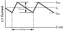
LM5575-Q1 30070810.gifFigure 17. Inductor Current Waveform

To keep the circuit in CCM, the maximum ripple current IRIPPLE must be less than twice the minimum load current, or 0.4 Ap-p. Using this value of ripple current, the value of inductor (L1) is calculated using Equation 8 and Equation 9:

Equation 8. LM5575-Q1 30070811.gif
Equation 9. LM5575-Q1 30070812.gif

This procedure provides a guide to select the value of L1. The nearest standard value (47 µH) is used. L1 must be rated for the peak current (IPK+) to prevent saturation. During normal loading conditions, the peak current occurs at maximum load current plus maximum ripple. During an overload condition, the peak current is limited to 2.1 A nominal (2.5 A maximum). The selected inductor has a conservative 3.25-Amp saturation current rating. The saturation rating is defined by inductor manufacturers as the current necessary for the inductance to reduce by 30%, at 20°C.