ZHCSTL7I February 2007 – November 2023 LM5116
PRODUCTION DATA
- 1
- 1 特性
- 2 应用
- 3 说明
- 4 Pin Configuration and Functions
- 5 Specifications
- 6 Detailed Description
-
7 Application and Implementation
- 7.1 Application Information
- 7.2
Typical Application
- 7.2.1 Design Requirements
- 7.2.2
Detailed Design Procedure
- 7.2.2.1 Custom Design with WEBENCH® Tools
- 7.2.2.2 Timing Resistor
- 7.2.2.3 Output Inductor
- 7.2.2.4 Current Sense Resistor
- 7.2.2.5 Ramp Capacitor
- 7.2.2.6 Output Capacitors
- 7.2.2.7 Input Capacitors
- 7.2.2.8 VCC Capacitor
- 7.2.2.9 Bootstrap Capacitor
- 7.2.2.10 Soft Start Capacitor
- 7.2.2.11 Output Voltage Divider
- 7.2.2.12 UVLO Divider
- 7.2.2.13 MOSFETs
- 7.2.2.14 MOSFET Snubber
- 7.2.2.15 Error Amplifier Compensation
- 7.2.2.16 Comprehensive Equations
- 7.2.3 Application Curves
- 7.3 Power Supply Recommendations
- 7.4 Layout
- 8 Device and Documentation Support
- 9 Revision History
- 10Mechanical, Packaging, and Orderable Information
7.2.2.6 Output Capacitors
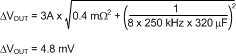
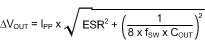
The output capacitors smooth the inductor ripple current and provide a source of charge for transient loading conditions. For this design example, five 100-µF ceramic capacitors where selected. Ceramic capacitors provide very low equivalent series resistance (ESR), but can exhibit a significant reduction in capacitance with DC bias. From the manufacturer’s data, the ESR at 250 kHz is 2 mΩ / 5 = 0.4 mΩ, with a 36% reduction in capacitance at 5 V. This is verified by measuring the output ripple voltage and frequency response of the circuit. The fundamental component of the output ripple voltage is calculated as:
With typical values for the 5-V design example: