SNVS269D January 2004 – December 2014 LM5104
PRODUCTION DATA.
8 Application and Implementation
NOTE
Information in the following applications sections is not part of the TI component specification, and TI does not warrant its accuracy or completeness. TI’s customers are responsible for determining suitability of components for their purposes. Customers should validate and test their design implementation to confirm system functionality.
8.1 Application Information
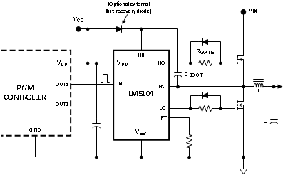
The LM5104 is one of the latest generation of high-voltage gate drivers which are designed to drive both the high-side and low-side N-channel MOSFETs in a half-bridge/full bridge configuration or in a synchronous buck circuit. The floating high-side driver can operate with supply voltages up to 100 V. This allows for N-channel MOSFET control in half-bridge, full-bridge, push-pull, two switch forward and active clamp topologies.
Table 1. Highlights
| FEATURE | BENEFIT |
|---|---|
| Adaptive Rising and Falling Edges with Programmable Additional Delay | Allows optimization of gate drive timings to account for device differences between high-side and low-side positions. |
| Single Input Control | Direct drive from lower cost PWM controllers |
| Internal Bootstrap Diode | Reduces parts count and PCB real estate |
8.2 Typical Application
8.2.1 Design Requirements
| PARAMETER | VALUE |
|---|---|
| Gate Driver IC | LM5104 |
| Mosfet | CSD18531Q5A |
| VDD | 10 V |
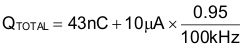
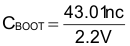
| Qgmax | 43 nC |
| Fsw | 200 kHz |
| DMax | 95% |
| IHBO | 10 µA |
| VDH | 1.1 V |
| VHBR | 7.1 V |
| VHBH | 0.4 V |
8.2.2 Detailed Design Procedure
where
- VDD = Supply voltage of the gate drive IC
- VDH = Bootstrap diode forward voltage drop
- Vgsmin = Minimum gate source threshold voltage
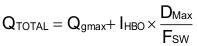
The quiescent current of the bootstrap circuit is 10 µA which is negligible compared to the Qgs of the MOSFET.
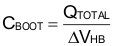
In practice the value for the CBOOT capacitor should be greater than that calculated to allow for situations where the power stage may skip pulse due to load transients. In this circumstance the boot capacitor must maintain the HB pin voltage above the UVLO voltage for the HB circuit.
As a general rule the local VDD bypass capacitor should be 10 times greater than the value of CBOOT.
The bootstrap and bias capacitors should be ceramic types with X7R dielectric. The voltage rating should be twice that of the maximum VDD to allow for loss of capacitance once the devices have a DC bias voltage across them and to ensure long-term reliability of the devices.
An additional delay turn-on delay can be programmed using an external resistor, RT. Figure 17 shows the relationship between the turnon delay time and the resistor value for RT.
8.2.3 Application Curves
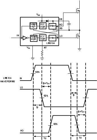 Figure 16. Application Timing Waveforms
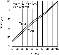 Figure 17. Turn On Delay vs RT Resistor Value