SNVS269D January 2004 – December 2014 LM5104
PRODUCTION DATA.
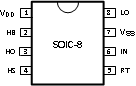
5 Pin Configuration and Functions
D Package
8-Pin SOIC
Top View
DPR Package
10-Pin WSON
Top View
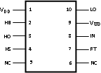
Pin Functions
| PIN | NAME | DESCRIPTION | APPLICATION INFORMATION | |
|---|---|---|---|---|
| SOIC | WSON | |||
| 1 | 1 | VDD | Positive gate drive supply | Locally decouple to VSS using ESR/ESL capacitor, located as close to IC as possible. |
| 2 | 2 | HB | High-side gate driver bootstrap rail | Connect the positive terminal to bootstrap capacitor to the HB pin and connect negative terminal to HS. The Bootstrap capacitor should be placed as close to IC as possible |
| 3 | 3 | HO | High-side gate driver output | Connect to gate of high-side MOSFET with short low inductance path. |
| 4 | 4 | HS | High-side MOSFET source connection | Connect to bootstrap capacitor negative terminal and source of high-side MOSFET. |
| 5 | 7 | RT | Deadtime programming pin | Resistor from RT to ground programs the deadtime between high- and low-side transitions. The resistor should be located close to the IC to minimize noise coupling from adjacent traces. |
| 6 | 8 | IN | Control input | Logic 1 equals High-side ON and Low-side OFF. Logic 0 equals High-side OFF and Low-side ON. |
| 7 | 9 | VSS | Ground return | All signals are referenced to this ground. |
| 8 | 10 | LO | Low-side gate driver output | Connect to the gate of the low-side MOSFET with a short low inductance path. |