ZHCSES8 March 2016 LM5022-Q1
PRODUCTION DATA.
- 1 特性
- 2 应用
- 3 说明
- 4 修订历史记录
- 5 Pin Configuration and Functions
- 6 Specifications
- 7 Detailed Description
-
8 Application and Implementation
- 8.1 Application Information
- 8.2
Typical Application
- 8.2.1 Design Requirements
- 8.2.2
Detailed Design Procedure
- 8.2.2.1 Switching Frequency
- 8.2.2.2 MOSFET
- 8.2.2.3 Output Diode
- 8.2.2.4 Boost Inductor
- 8.2.2.5 Output Capacitor
- 8.2.2.6 VCC Decoupling Capacitor
- 8.2.2.7 Input Capacitor
- 8.2.2.8 Current Sense Filter
- 8.2.2.9 RSNS, RS2 and Current Limit
- 8.2.2.10 Control Loop Compensation
- 8.2.2.11 Efficiency Calculations
- 8.2.3 Application Curves
- 9 Power Supply Recommendations
- 10Layout
- 11器件和文档支持
- 12机械、封装和可订购信息
10 Layout
10.1 Layout Guidelines
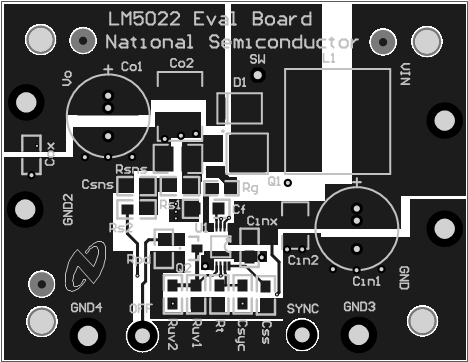
To produce an optimal power solution with the LM5022-Q1, good layout and design of the PCB are as critical as component selection. The following are the several guidelines in order to create a good layout of the PCB, as based on Figure 15.
- Using a low ESR ceramic capacitor, place CINX as close as possible to the VIN and GND pins of the LM5022-Q1.
- Using a low ESR ceramic capacitor, place COX close to the load as possible of the LM5022-Q1
- Using a low ESR ceramic capacitor place CF close to the VCC and GND pins of the LM5022-Q1
- Minimize the loop area formed by the output capacitor connections (Co1, Co2 ), by D1 and Rsns. Making sure the cathode of D1 and Rsns are position next to each other and place Co1(+ )and Co1( -) close to D1 cathode and Rsns (-) respectively.
- Rsns (+) should be connected to the CS pin with a separate trace made as short as possible. This trace should be routed away from the inductor and the switch node (where D1, Q1, and L1 connect).
- Minimize the trace length to the FB pin by positioning RFB1 and RFB2 close to the LM5022-Q1
- Route the VOUT sense path away from noisy node and connect it as close as possible to the positive side of COX.
10.1.1 Filter Capacitors
The low-value ceramic filter capacitors are most effective when the inductance of the current loops that they filter, is minimized. Place CINX as close as possible to the VIN and GND pins of the LM5022-Q1. Place COX close to the load, and CF next to the VCC and GND pins of the LM5022-Q1.
10.1.2 Sense Lines
The top of RSNS should be connected to the CS pin with a separate trace, made as short as possible. Route this trace away from the inductor and the switch node (where D1, Q1, and L1 connect). For the voltage loop, keep RFB1and RFB2 close to the LM5022-Q1 and run a trace, as close as possible, to the positive side of COX to RFB2. As with the CS line, the FB line should be routed away from the inductor and the switch node. These measures minimize the length of high impedance lines and reduce noise pickup.
10.1.3 Compact Layout
- Parasitic inductance can be reduced by keeping the power path components close together. As described above in point 4 in the Layout Guidelines, keep the high slew-rate current loops as tight as possible. Short, thick traces or copper pours (shapes) are best
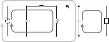
- The switch node should be just large enough to connect all the components together without excessive heating from the current it carries. The LM5022-Q1 (boost converter) operates in two distinct cycles whose high current paths are shown in Figure 30:
 Figure 30. Boost Converter Current Loops
The dark grey, inner loops represent the high current paths during the MOSFET on-time. The light grey, outer loop represents the high current path during the off-time.
10.1.4 Ground Plane and Shape Routing
The diagram of Figure 30 is useful for analyzing the flow of continuous current vs. the flow of pulsating currents. The circuit paths with current flow during both the on-time and off-time are considered to be continuous current, while those that carry current during the on-time or off-time only are pulsating currents. Preference in routing should be given to the pulsating current paths, as these are the portions of the circuit most likely to emit EMI. The ground plane of a PCB is a conductor and return path, and it is susceptible to noise injection just as any other circuit path. The continuous current paths on the ground net can be routed on the system ground plane with less risk of injecting noise into other circuits. The path between the input source, input capacitor and the MOSFET and the path between the output capacitor and the load are examples of continuous current paths. In contrast, the path between the grounded side of the power switch and the negative output capacitor terminal carries a large high slew-rate pulsating current. This path should be routed with a short, thick shape, preferably on the component side of the PCB. Too keep the parasitic inductance low, multiple vias in parallel should be placed on the negative pads of the input and output capacitors to connect the component side to the ground plane. Vias should not be placed directly at the grounded side of the MOSFET (or RSNS) as they tend to inject noise into the ground plane. A second pulsating current loop is the gate drive loop formed by the OUT and VCC pins, Q1, RSNS and capacitor CF. These loops must be kept small.
10.2 Layout Example
 Figure 31. Typical Top Layer Overlay of the LM5022 Evaluation Board
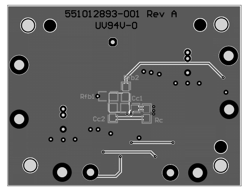
 Figure 32. Typical Bottom Layer Overlay of the LM5022 Evaluation Board