SNVS484H January 2007 – July 2015 LM5001 , LM5001-Q1
PRODUCTION DATA.
- 1 Features
- 2 Applications
- 3 Description
- 4 Revision History
- 5 Pin Configuration and Functions
- 6 Specifications
- 7 Detailed Description
- 8 Applications and Implementation
- 9 Layout
- 10Device and Documentation Support
- 11Mechanical, Packaging, and Orderable Information
5 Pin Configuration and Functions
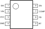
SOIC (D) 8 Pins
Top View

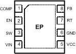
WSON (NGT) 8 Pins
Top View

Pin Functions
| PIN | NAME | TYPE | DESCRIPTION | |
|---|---|---|---|---|
| SOIC | WSON | |||
| 1 | 3 | SW | Switch pin | The drain terminal of the internal power MOSFET. |
| 2 | 4 | VIN | Input supply pin | Nominal operating range: 3.1 V to 75 V. |
| 3 | 5 | VCC | Bias regulator output, or input for external bias supply | VCC tracks VIN up to 6.9 V. Above VIN = 6.9 V, VCC is regulated to 6.9 V. A 0.47-µF or greater ceramic decoupling capacitor is required. An external voltage (7 V – 12 V) can be applied to this pin which disables the internal VCC regulator to reduce internal power dissipation and improve converter efficiency. |
| 4 | 6 | GND | Ground | Internal reference for the regulator control functions and the power MOSFET current sense resistor connection. |
| 5 | 7 | RT | Oscillator frequency programming and optional synchronization pulse input | The internal oscillator is set with a resistor, between this pin and the GND pin. The recommended frequency range is 50 KHz to 1.5 MHz. The RT pin can accept synchronization pulses from an external clock. A 100-pF capacitor is recommended for coupling the synchronizing clock to the RT pin. |
| 6 | 8 | FB | Feedback input from the regulated output voltage | This pin is connected to the inverting input of the internal error amplifier. The 1.26-V reference is internally connected to the non-inverting input of the error amplifier. |
| 7 | 1 | COMP | Open drain output of the internal error amplifier | The loop compensation network should be connected between the COMP pin and the FB pin. COMP pull-up is provided by an internal 5-kΩ resistor which may be used to bias an opto-coupler transistor (while FB is grounded) for isolated ground applications. |
| 8 | 2 | EN | Enable / Undervoltage Lock-Out / Shutdown input | An external voltage divider can be used to set the line undervoltage lockout threshold. If the EN pin is left unconnected, a 6-µA pull-up current source pulls the EN pin high to enable the regulator. |
| NA | EP | EP | Exposed Pad, WSON only | Exposed metal pad on the underside of the package with a resistive connection to pin 6. It is recommended to connect this pad to the PC board ground plane in order to improve heat dissipation. |