SLOS456N January 2005 – October 2017
PRODUCTION DATA.
- 1 Features
- 2 Applications
- 3 Description
- 4 Revision History
- 5 Pin Configuration and Functions
-
6 Specifications
- 6.1 Absolute Maximum Ratings
- 6.2 ESD Ratings
- 6.3 Recommended Operating Conditions
- 6.4 Thermal Information
- 6.5 LM4040A20I, LM4040B20I Electrical Characteristics
- 6.6 LM4040C20I, LM4040D20I Electrical Characteristics
- 6.7 LM4040C20Q, LM4040D20Q Electrical Characteristics
- 6.8 LM4040A25I, LM4040B25I Electrical Characteristics
- 6.9 LM4040C25I, LM4040D25I Electrical Characteristics
- 6.10 LM4040C25Q, LM4040D25Q Electrical Characteristics
- 6.11 LM4040A30I, LM4040B30I Electrical Characteristics
- 6.12 LM4040C30I, LM4040D30I Electrical Characteristics
- 6.13 LM4040C30Q, LM4040D30Q Electrical Characteristics
- 6.14 LM4040A41I, LM4040B41I Electrical Characteristics
- 6.15 LM4040C41I, LM4040D41I Electrical Characteristics
- 6.16 LM4040A50I, LM4040B50I Electrical Characteristics
- 6.17 LM4040C50I, LM4040D50I Electrical Characteristics
- 6.18 LM4040C50Q, LM4040D50Q Electrical Characteristics
- 6.19 LM4040A82I, LM4040B82I Electrical Characteristics
- 6.20 LM4040C82I, LM4040D82I Electrical Characteristics
- 6.21 LM4040A10I, LM4040B10I Electrical Characteristics
- 6.22 LM4040C10I, LM4040D10I Electrical Characteristics
- 6.23 Typical Characteristics
- 7 Detailed Description
- 8 Applications and Implementation
- 9 Power Supply Recommendations
- 10Layout
- 11Device and Documentation Support
- 12Mechanical, Packaging, and Orderable Information
封装选项
机械数据 (封装 | 引脚)
散热焊盘机械数据 (封装 | 引脚)
订购信息
8 Applications and Implementation
NOTE
Information in the following applications sections is not part of the TI component specification, and TI does not warrant its accuracy or completeness. TI’s customers are responsible for determining suitability of components for their purposes. Customers should validate and test their design implementation to confirm system functionality.
8.1 Application Information
LM4040 is a well known industry standard device used in several applications and end equipment where a reference is required. Below describes this device being used in a data acquisition system. Analog to Digital conversion systems are the most common applications to use LM4040 due to its low reference tolerance which allows high precision in these systems.
8.2 Typical Applications
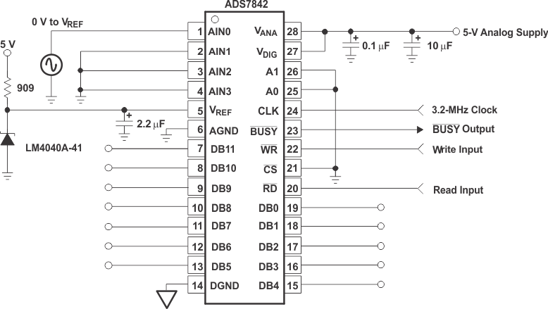
 Figure 6. Data-Acquisition Circuit With LM4040x-41
8.2.1 Design Requirements
For this design example, use the parameters listed in Table 1 as the input parameters.
Table 1. Design Parameters
| DESIGN PARAMETER | EXAMPLE VALUE |
|---|---|
| ADC FSR (Full Scale Range) | 4.096 |
| ADC Resolution | 12 Bits |
| Supply Voltage | 5 V |
| Cathode Current (Ik) | 100 µA |
8.2.2 Detailed Design Procedure
When using LM4040 as a comparator with reference, determine the following:
- Input voltage range
- Reference voltage accuracy
- Output logic input high and low level thresholds
- Current source resistance
8.2.2.1 LM4040 Voltage and Accuracy Choice
When using LM4040 as a reference for an ADC, the ADC's FSR (Full Scale Range), Resolution and LSB must be determined. LSB can be determined by:
LSB=FSR/(2N-1)
With N being the resolution or Number of Bits. FSR and Resolution can be determined by the ADC's datasheet.
Vref can be determined by:
Vref=FSR+LSB
Though modern data converters use calibration techniques to compensate for any error introduced by a Vref's inaccuracy, it is best to use the highest accuracy available. This is due to errors in the calibration method that may allow some non-linearities introduced by the Vref's initial accuracy.
A good example is the LM4040x-41 that is designed to be a cost-effective voltage reference as required in 12-bit data-acquisition systems. For 12-bit systems operating from 5-V supplies (see Figure 6), the LM4040A-41 (4.096 V, 0.01%) only introduces 4 LSBs (4mV) of possible error in a system that consists of 4096 LSBs.
8.2.2.2 Cathode and Load Currents
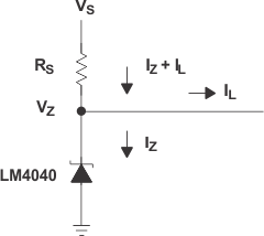
In a typical shunt-regulator configuration (see Figure 7), an external resistor, RS, is connected between the supply and the cathode of the LM4040. RS must be set properly, as it sets the total current available to supply the load (IL) and bias the LM4040 (IZ). In all cases, IZ must stay within a specified range for proper operation of the reference. Taking into consideration one extreme in the variation of the load and supply voltage (maximum IL and minimum VS), RS must be small enough to supply the minimum IZ required for operation of the regulator, as given by data-sheet parameters. At the other extreme, maximum VS and minimum IL, RS must be large enough to limit IZ to less than its maximum-rated value of 15 mA.
RS is calculated according to Equation 1:

 Figure 7. Shunt Regulator
8.2.2.3 Output Capacitor
The LM4040 does not require an output capacitor across cathode and anode for stability. However, if an output bypass capacitor is desired, the LM4040 is designed to be stable with all capacitive loads.
8.2.2.4 SOT-23 Connections
There is a parasitic Schottky diode connected between pins 2 and 3 of the SOT-23 packaged device. Thus, pin 3 of the SOT-23 package must be left floating or connected to pin 2.
8.2.2.5 Start-Up Characteristics
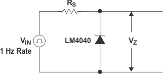
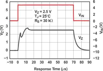
In any data conversion system, start-up characteristics are important, as to determine when it is safe begin conversion based upon a steady and settled reference value. As shown in Figure 9 it is best to allow for >20µs from supply start-up to begin conversion.
 Figure 8. Test Circuit
8.2.3 Application Curve
 Figure 9. Startup Response