ZHCSIW6L October 2000 – October 2018 LM4040-N , LM4040-N-Q1
PRODUCTION DATA.
- 1 特性
- 2 应用
- 3 说明
- 4 修订历史记录
- 5 Pin Configuration and Functions
-
6 Specifications
- 6.1 Absolute Maximum Ratings
- 6.2 ESD Ratings
- 6.3 Recommended Operating Conditions
- 6.4 Thermal Information
- 6.5 Electrical Characteristics: 2-V LM4040-N VR Tolerance Grades 'A' And 'B'; Temperature Grade 'I'
- 6.6 Electrical Characteristics: 2-V LM4040-N VR Tolerance Grades 'C', 'D', And 'E'; Temperature Grade 'I'
- 6.7 Electrical Characteristics: 2-V LM4040-N VR Tolerance Grades 'C', 'D', And 'E'; Temperature Grade 'E'
- 6.8 Electrical Characteristics: 2.5-V LM4040-N VR Tolerance Grades 'A' And 'B'; Temperature Grade 'I' (AEC Grade 3)
- 6.9 Electrical Characteristics: 2.5-V LM4040-N VR Tolerance Grades 'C', 'D', and 'E'; Temperature Grade 'I' (AEC Grade 3)
- 6.10 Electrical Characteristics: 2.5-V LM4040-N VR Tolerance Grades 'C', 'D', And 'E'; Temperature Grade 'E' (AEC Grade 1)
- 6.11 Electrical Characteristics: 3-V LM4040-N VR Tolerance Grades 'A' And 'B'; Temperature Grade 'I'
- 6.12 Electrical Characteristics: 3-V LM4040-N VR Tolerance Grades 'C', 'D', And 'E'; Temperature Grade 'I'
- 6.13 Electrical Characteristics: 3-V LM4040-N VR Tolerance Grades 'C', 'D', And 'E'; Temperature Grade 'E'
- 6.14 Electrical Characteristics: 4.1-V LM4040-N VR Tolerance Grades 'A' And 'B'; Temperature Grade 'I'
- 6.15 Electrical Characteristics: 4.1-V LM4040-N VR Tolerance Grades 'C' and 'D'; Temperature Grade 'I'
- 6.16 Electrical Characteristics: 5-V LM4040-N VR Tolerance Grades 'A' And 'B'; Temperature Grade 'I'
- 6.17 Electrical Characteristics: 5-V LM4040-N VR Tolerance Grades 'C' And 'D'; Temperature Grade 'I'
- 6.18 Electrical Characteristics: 5-V LM4040-N VR Tolerance Grades 'C' And 'D'; Temperature Grade 'E'
- 6.19 Electrical Characteristics: 8.2-V LM4040-N VR Tolerance Grades 'A' And 'B'; Temperature Grade 'I'
- 6.20 Electrical Characteristics: 8.2-V Lm4040-N VR Tolerance Grades 'C' And 'D'; Temperature Grade 'I'
- 6.21 Electrical Characteristics: 10-V LM4040-N VR Tolerance Grades 'A' And 'B'; Temperature Grade 'I'
- 6.22 Electrical Characteristics: 10-V LM4040-N VR Tolerance Grades 'C' And 'D'; Temperature Grade 'I'
- 6.23 Typical Characteristics
- 7 Parameter Measurement Information
- 8 Detailed Description
- 9 Application and Implementation
- 10Power Supply Recommendations
- 11Layout
- 12器件和文档支持
- 13机械、封装和可订购信息
封装选项
机械数据 (封装 | 引脚)
散热焊盘机械数据 (封装 | 引脚)
订购信息
9.1 Application Information
The LM4040-N is a precision micropower curvature-corrected bandgap shunt voltage reference. For space critical applications, the LM4040-N is available in SOT-23 and SC70 surface-mount packages. The LM4040-N has been designed for stable operation without the need of an external capacitor connected between the + pin and the − pin. If, however, a bypass capacitor is used, the LM4040-N remains stable. Reducing design effort is the availability of several fixed reverse breakdown voltages: 2.048 V, 2.5 V, 3 V, 4.096 V, 5 V, 8.192 V, and 10 V. The minimum operating current increases from 60 µA for the LM4040-N-2.048 and LM4040-N-2.5 to 100 μA for the 10-V LM4040-N. All versions have a maximum operating current of 15 mA.
LM4040-Ns in the SOT-23 packages have a parasitic Schottky diode between pin 2 (−) and pin 3 (Die attach interface contact). Therefore, pin 3 of the SOT-23 package must be left floating or connected to pin 2.
LM4040-Ns in the SC70 have a parasitic Schottky diode between pin 1 (−) and pin 2 (Die attach interface contact). Therefore, pin 2 must be left floating or connected to pin1.
The 4.096-V version allows single 5-V 12-bit ADCs or DACs to operate with an LSB equal to 1 mV. For 12-bit ADCs or DACs that operate on supplies of 10 V or greater, the 8.192-V version gives 2 mV per LSB.
The typical thermal hysteresis specification is defined as the change in 25°C voltage measured after thermal cycling. The device is thermal cycled to temperature –40°C and then measured at 25°C. Next the device is thermal cycled to temperature 125°C and again measured at 25°C. The resulting VOUT delta shift between the 25°C measurements is thermal hysteresis. Thermal hysteresis is common in precision references and is induced by thermal-mechanical package stress. Changes in environmental storage temperature, operating temperature and board mounting temperature are all factors that can contribute to thermal hysteresis.
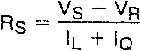
In a conventional shunt regulator application (Figure 10) , an external series resistor (RS) is connected between the supply voltage and the LM4040-N. RS determines the current that flows through the load (IL) and the LM4040-N (IQ). Since load current and supply voltage may vary, RS should be small enough to supply at least the minimum acceptable IQ to the LM4040-N even when the supply voltage is at its minimum and the load current is at its maximum value. When the supply voltage is at its maximum and IL is at its minimum, RS should be large enough so that the current flowing through the LM4040-N is less than 15 mA.
RS is determined by the supply voltage, (VS), the load and operating current, (IL and IQ), and the LM4040-N's reverse breakdown voltage, VR.
