SNVS434M July   2006  – November 2016 LM3673

PRODUCTION DATA.  

  1. Features
  2. Applications
  3. Description
  4. Revision History
  5. Voltage Options
  6. Pin Configuration and Functions
  7. Specifications
    1. 7.1 Absolute Maximum Ratings
    2. 7.2 ESD Ratings
    3. 7.3 Recommended Operating Ratings
    4. 7.4 Thermal Information
    5. 7.5 Electrical Characteristics
    6. 7.6 Typical Characteristics
  8. Detailed Description
    1. 8.1 Overview
    2. 8.2 Functional Block Diagram
    3. 8.3 Feature Description
      1. 8.3.1 Circuit Operation
      2. 8.3.2 PWM Operation
      3. 8.3.3 Internal Synchronous Rectification
      4. 8.3.4 Current Limiting
      5. 8.3.5 Soft Start
      6. 8.3.6 Low Drop Out Operation (LDO)
    4. 8.4 Device Functional Modes
      1. 8.4.1 PFM Operation
      2. 8.4.2 Shutdown Mode
  9. Application and Implementation
    1. 9.1 Application Information
    2. 9.2 Typical Applications
      1. 9.2.1 Design Requirements
      2. 9.2.2 Detailed Design Procedure
        1. 9.2.2.1 Output Voltage Selection for LM3673-ADJ
        2. 9.2.2.2 Inductor Selection
          1. 9.2.2.2.1 Method 1
          2. 9.2.2.2.2 Method 2
        3. 9.2.2.3 Input Capacitor Selection
        4. 9.2.2.4 Output Capacitor Selection
      3. 9.2.3 Application Curves
  10. 10Power Supply Recommendations
  11. 11Layout
    1. 11.1 Layout Guidelines
    2. 11.2 Layout Example
    3. 11.3 DSBGA Package Assembly and Use
  12. 12Device and Documentation Support
    1. 12.1 Device Support
      1. 12.1.1 Third-Party Products Disclaimer
    2. 12.2 Documentation Support
      1. 12.2.1 Related Documentation
    3. 12.3 Receiving Notification of Documentation Updates
    4. 12.4 Community Resources
    5. 12.5 Trademarks
    6. 12.6 Electrostatic Discharge Caution
    7. 12.7 Glossary
  13. 13Mechanical, Packaging, and Orderable Information

封装选项

机械数据 (封装 | 引脚)
散热焊盘机械数据 (封装 | 引脚)
订购信息

Pin Configuration and Functions

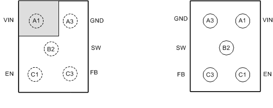
YZR Package
5-Pin DSBGA
Top (Left) and Bottom (Right) Views
LM3673 20183344.gif

Pin Functions

PIN I/O DESCRIPTION
NUMBER NAME
A1 VIN Power Power supply input. Connect to the input filter capacitor (Figure 17).
A3 GND Ground Ground pin
B2 SW Analog Switching node connection to the internal PFET switch and NFET synchronous rectifier.
C1 EN Input Enable pin. The device is in shutdown mode when voltage to this pin is < 0.4 V and enabled when > 1 V. Do not leave this pin floating.
C3 FB Analog Feedback analog input. Connect directly to the output filter capacitor for fixed voltage versions. For adjustable version external resistor dividers are required (Figure 18). The internal resistor dividers are disabled for the adjustable version.