SNVS250F November   2004  – February 2016 LM3670

PRODUCTION DATA.  

  1. Features
  2. Applications
  3. Description
  4. Revision History
  5. Connection Diagram
  6. Specifications
    1. 6.1 Absolute Maximum Ratings
    2. 6.2 ESD Ratings
    3. 6.3 Recommended Operating Conditions
    4. 6.4 Thermal Information
    5. 6.5 Electrical Characteristics
    6. 6.6 Typical Characteristics
  7. Detailed Description
    1. 7.1 Overview
    2. 7.2 Functional Block Diagram
    3. 7.3 Feature Description
      1. 7.3.1 Circuit Operation
      2. 7.3.2 Soft Start
      3. 7.3.3 LDO - Low Dropout Operation
    4. 7.4 Device Functional Modes
      1. 7.4.1 PWM Operation
        1. 7.4.1.1 Internal Synchronous Rectification
        2. 7.4.1.2 Current Limiting
      2. 7.4.2 PFM Operation
      3. 7.4.3 Shutdown
  8. Application and Implementation
    1. 8.1 Application Information
    2. 8.2 Typical Application
      1. 8.2.1 Typical Application: Fixed Output
        1. 8.2.1.1 Design Requirements
        2. 8.2.1.2 Detailed Design Procedure
          1. 8.2.1.2.1 Inductor Selection
            1. 8.2.1.2.1.1 Method 1
            2. 8.2.1.2.1.2 Method 2
          2. 8.2.1.2.2 Input Capacitor Selection
          3. 8.2.1.2.3 Output Capacitor Selection
        3. 8.2.1.3 Application Curves
      2. 8.2.2 Typical Application: Adjustable Output
        1. 8.2.2.1 Design Requirements
        2. 8.2.2.2 Detailed Design Procedure
          1. 8.2.2.2.1 Output Voltage Selection for Adjustable LM3670
        3. 8.2.2.3 Application Curves
  9. Power Supply Recommendations
  10. 10Layout
    1. 10.1 Layout Guidelines
    2. 10.2 Layout Example
  11. 11Device and Documentation Support
    1. 11.1 Device Support
      1. 11.1.1 Third-Party Products Disclaimer
    2. 11.2 Community Resources
    3. 11.3 Trademarks
    4. 11.4 Electrostatic Discharge Caution
    5. 11.5 Glossary
  12. 12Mechanical, Packaging, and Orderable Information

封装选项

机械数据 (封装 | 引脚)
散热焊盘机械数据 (封装 | 引脚)
订购信息

5 Connection Diagram

DBV Package
5-Pin SOT-23
Top View
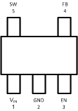
LM3670 20075802.gif

Pin Functions

PIN TYPE DESCRIPTION
NUMBER NAME
1 VIN Power Power supply input. Connect to the input filter capacitor
( Typical Application: Fixed Output).
2 GND Ground Ground pin.
3 EN Digital Enable input.
4 FB Analog Feedback analog input. Connect to the output filter capacitor
(Typical Application: Fixed Output).
5 SW Analog Switching node connection to the internal PFET switch and NFET synchronous rectifier. Connect to an inductor with a saturation current rating that exceeds the 750-mA maximum switch peak current limit specification.