SNVS780E May 1998 – December 2016 LM337L
PRODUCTION DATA.
8 Application and Implementation
NOTE
Information in the following applications sections is not part of the TI component specification, and TI does not warrant its accuracy or completeness. TI’s customers are responsible for determining suitability of components for their purposes. Customers should validate and test their design implementation to confirm system functionality.
8.1 Application Information
The LM337L is a negative output linear regulator with high accuracy and a wide temperature range. An output capacitor can be added to further improve transient response, and the ADJ pin can be bypassed to achieve very high ripple-rejection ratios. The device's functionality can be utilized in many different applications that require negative voltage supplies, such as bipolar amplifiers, operational amplifiers, and constant current regulators.
8.2 Typical Applications
8.2.1 1.2-V to 25-V Adjustable Regulator

8.2.1.1 Design Requirements
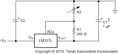
The device component count is very minimal, employing two resistors as part of a voltage divider circuit and an output capacitor for load regulation. An input capacitor is needed if the device is more than 4 in. from the filter capacitors.
8.2.1.2 Detailed Design Procedure
The output voltage is set based on the selection of the two resistors (R1 and R2) as shown in Equation 1.

8.2.1.3 Application Curve
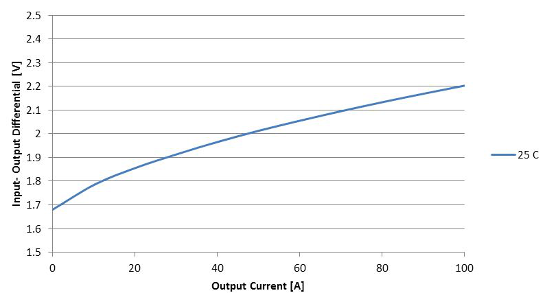
 Figure 7. Dropout Voltage across Load Current at 25°C (∆Vout < 100 mV
8.2.2 Regulator With Trimmable Output Voltage
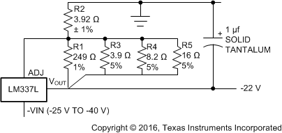
 Figure 8. Regulator with Trimmable Output Voltage Diagram
8.2.2.1 Design Requirements
This design uses five resistors with two being used for a voltage divider circuit and the other three used for trimming the output voltage. The benefit is lower cost as compared to using a trim pot. An output capacitor is needed to improve load regulation.
8.2.2.2 Detailed Design Procedure
This design will trim the output voltage to within 1% of –22 V. The parallel combination of R1, R3, R4 and R5 serve as the bottom resistance and R2 as the top resistance in the voltage divider that sets the output voltage.
Trim Procedure:
- If VOUT is –23.08 V or larger, do not use R3, otherwise leave it in.
- Then if VOUT is –22.47 V or bigger, do not use R4, otherwise leave it in.
- Then if VOUT is –22.16 V or bigger, do not use R5, otherwise leave it in.