ZHCSGH7 June 2017 LM324-MIL
PRODUCTION DATA.
8 Detailed Description
8.1 Overview
The device consists of four independent high-gain frequency-compensated operational amplifiers that are designed specifically to operate from a single supply over a wide range of voltages. Operation from split supplies also is possible if the difference between the two supplies is 3 V to 32 V, and VCC is at least 1.5 V more positive than the input common-mode voltage. The low supply-current drain is independent of the magnitude of the supply voltage.
Applications include transducer amplifiers, DC amplification blocks, and all the conventional operational-amplifier circuits that now can be more easily implemented in single-supply-voltage systems. For example, the LM324-MIL device can be operated directly from the standard 5-V supply that is used in digital systems and provides the required interface electronics, without requiring additional ±15-V supplies.
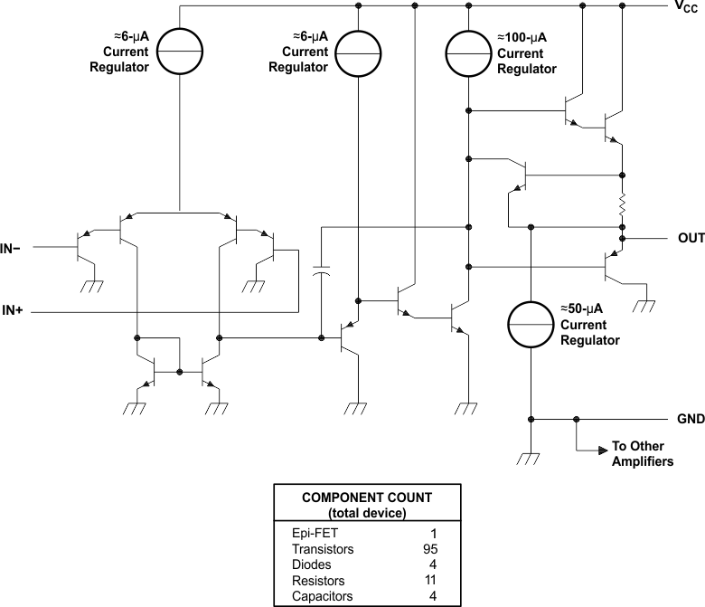
8.2 Functional Block Diagram

8.3 Feature Description
8.3.1 Unity-Gain Bandwidth
Gain bandwidth product is found by multiplying the measured bandwidth of an amplifier by the gain at which that bandwidth was measured. These devices have a high gain bandwidth of 1.2 MHz.
8.3.2 Slew Rate
The slew rate is the rate at which an operational amplifier can change its output when there is a change on the input. These devices have a 0.5-V/μs slew rate.
8.3.3 Input Common Mode Range
The valid common mode range is from device ground to VCC – 1.5 V (VCC – 2 V across temperature). Inputs may exceed VCC up to the maximum VCC without device damage. At least one input must be in the valid input common mode range for output to be correct phase. If both inputs exceed valid range then output phase is undefined. If either input is less than –0.3 V then input current should be limited to 1 mA and output phase is undefined.
8.4 Device Functional Modes
The device is powered on when the supply is connected. This device can be operated as a single supply operational amplifier or dual supply amplifier depending on the application.