ZHCS522H January 2006 – October 2017 LM3100
PRODUCTION DATA.
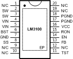
5 Pin Configuration and Functions
PWP Package
20-Pin HTSSOP
Top View

Pin Functions
| PIN | DESCRIPTION | ||
|---|---|---|---|
| NO. | NAME | ||
| 1,9,10,12,19,20 | N/C | No Connection These pins must be left unconnected. |
|
| 2, 3 | SW | Switching Node Internally connected to the buck switch source. Connect to output inductor. |
|
| 4, 5 | VIN | Input supply voltage Supply pin to the device. Nominal input range is 4.5 V to 36 V. |
|
| 6 | BST | Connection for bootstrap capacitor Connect a 0.033 µF capacitor from SW pin to this pin. An internal diode charges the capacitor during the high-side switch off-time. |
|
| 7 | GND | Analog Ground Ground for all internal circuitry other than the synchronous switches. |
|
| 8 | SS | Soft-start An internal 8 µA current source charges an external capacitor to provide the soft- start function. |
|
| 11 | TST | Test mode enable pin Force the device into test mode. Must be connected to ground for normal operation. |
|
| 13 | FB | Feedback Internally connected to the regulation and over-voltage comparators. The regulation setting is 0.8 V at this pin. Connect to feedback divider. |
|
| 14 | EN | Enable pin Connect a voltage higher than 1.26 V to enable the regulator. |
|
| 15 | RON | On-time Control An external resistor from VIN to this pin sets the high-side switch on-time. |
|
| 16 | VCC | Start-up regulator Output Nominally regulated to 6 V. Connect a capacitor of not less than 680 nF between VCC and GND for stable operation. |
|
| 17, 18 | PGND | Power Ground Synchronous rectifier MOSFET source connection. Tie to power ground plane. |
|
| DAP | EP | Exposed Pad Thermal connection pad, connect to GND. |
|