SNVS191F November 2002 – October 2016 LM2705
PRODUCTION DATA.
- 1 Features
- 2 Applications
- 3 Description
- 4 Revision History
- 5 Pin Configuration and Functions
- 6 Specifications
- 7 Detailed Description
- 8 Application and Implementation
- 9 Power Supply Recommendations
- 10Layout
- 11Device and Documentation Support
- 12Mechanical, Packaging, and Orderable Information
8 Application and Implementation
NOTE
Information in the following applications sections is not part of the TI component specification, and TI does not warrant its accuracy or completeness. TI’s customers are responsible for determining suitability of components for their purposes. Customers should validate and test their design implementation to confirm system functionality.
8.1 Application Information
The LM2705 is a 20-V boost designed for low power boost applications. Typical input voltage range makes this ideal for standard single cell Li+ batteries or 2 to 4 series alkaline batteries.
8.2 Typical Application
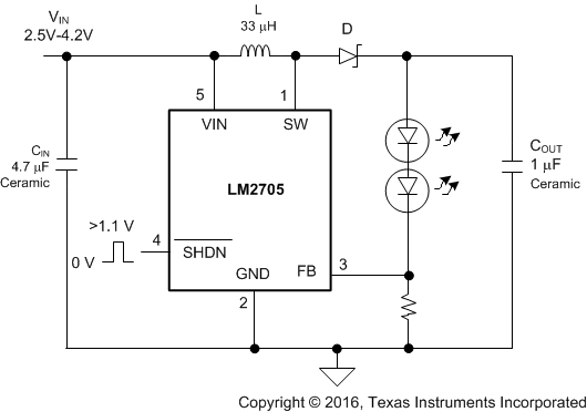
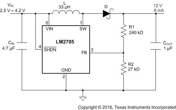
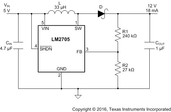
Figure 12 shows a typical Li+ voltage range to 20-V application. The 68-µH inductor allows for a low ripple current and high light-load efficiency.
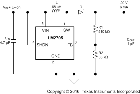 Figure 12. Typical 20-V Application
8.2.1 Design Requirements
For typical DC-DC converter applications, use the parameters listed in Table 1.
Table 1. Design Parameters
| DESIGN PARAMETER | EXAMPLE VALUE |
|---|---|
| Input voltage | 2.5 V to 4.2 V |
| Output voltage | 12 V |
| Output current | up to 8 mA |
| Inductor | 33 µH |
8.2.2 Detailed Design Procedure
8.2.2.1 Inductor Selection - Boost Regulator
The appropriate inductor for a given application is calculated using Equation 1:

where
- VD is the Schottky diode voltage
- ICL is the switch current limit found in the Typical Characteristics
- TOFF is the switch off time
When using this equation be sure to use the minimum input voltage for the application, such as for battery powered applications. For the LM2705 constant-off time control scheme, the NMOS power switch is turned off when the current limit is reached. There is approximately a 100-ns delay from the time the current limit is reached in the NMOS power switch and when the internal logic actually turns off the switch. During this 100-ns delay, the peak inductor current increases. This increase in inductor current demands a larger saturation current rating for the inductor. This saturation current can be approximated by Equation 2:

Choosing inductors with low ESR decrease power losses and increase efficiency.
Take care when choosing an inductor. For applications that require an input voltage that approaches the output voltage, such as when converting a Li-Ion battery voltage to 5 V, the 400-ns off time may not be enough time to discharge the energy in the inductor and transfer the energy to the output capacitor and load. This can cause a ramping effect in the inductor current waveform and an increased ripple on the output voltage. Using a smaller inductor causes the IPK to increase and increases the output voltage ripple further.
For typical curves and evaluation purposes the DT1608C series inductors from Coilcraft were used. Other acceptable inductors include, but are not limited to, the SLF6020T series from TDK, the NP05D series from Taiyo Yuden, the CDRH4D18 series from Sumida, and the P1166 series from Pulse.
8.2.2.2 Inductor Selection - SEPIC Regulator
Equation 3 can be used to calculate the approximate inductor value for a SEPIC regulator:

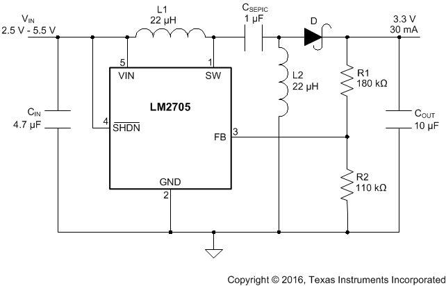
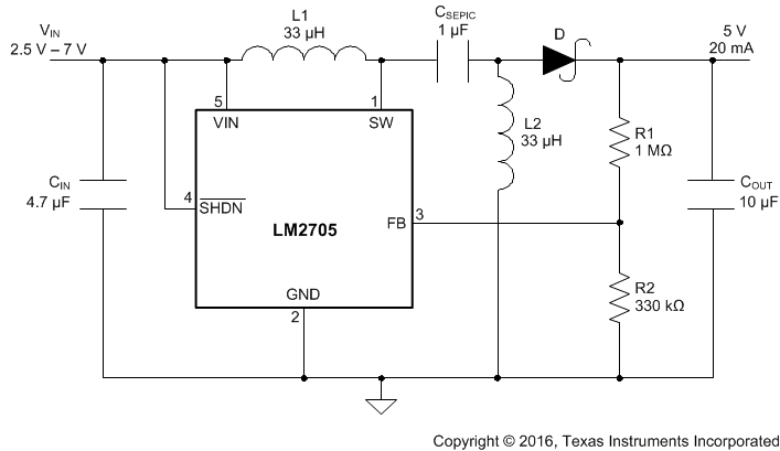
The boost inductor, L1, can be smaller or larger but is generally chosen to be the same value as L2. See Figure 23 and Figure 24 for typical SEPIC applications.
8.2.2.3 Diode Selection
To maintain high efficiency, the average current rating of the Schottky diode should be larger than the peak inductor current, IPK. Schottky diodes with a low forward drop and fast switching speeds are ideal for increasing efficiency in portable applications. Choose a reverse breakdown of the Schottky diode larger than the output voltage.
8.2.2.4 Capacitor Selection
Choose low equivalent series resistance (ESR) capacitors for the output to minimize output voltage ripple. Multilayer ceramic capacitors are the best choice. For most applications, a 1-µF ceramic capacitor is sufficient. For some applications a reduction in output voltage ripple can be achieved by increasing the output capacitor. Output voltage ripple can further be reduced by adding a 4.7-pF feed-forward capacitor in the feedback network placed in parallel with RF1 (see Functional Block Diagram).
Local bypassing for the input is needed on the LM2705. Multilayer ceramic capacitors are a good choice for this as well. A 4.7-µF capacitor is sufficient for most applications. For additional bypassing, a 100-nF ceramic capacitor can be used to shunt high frequency ripple on the input.
8.2.3 Application Curves
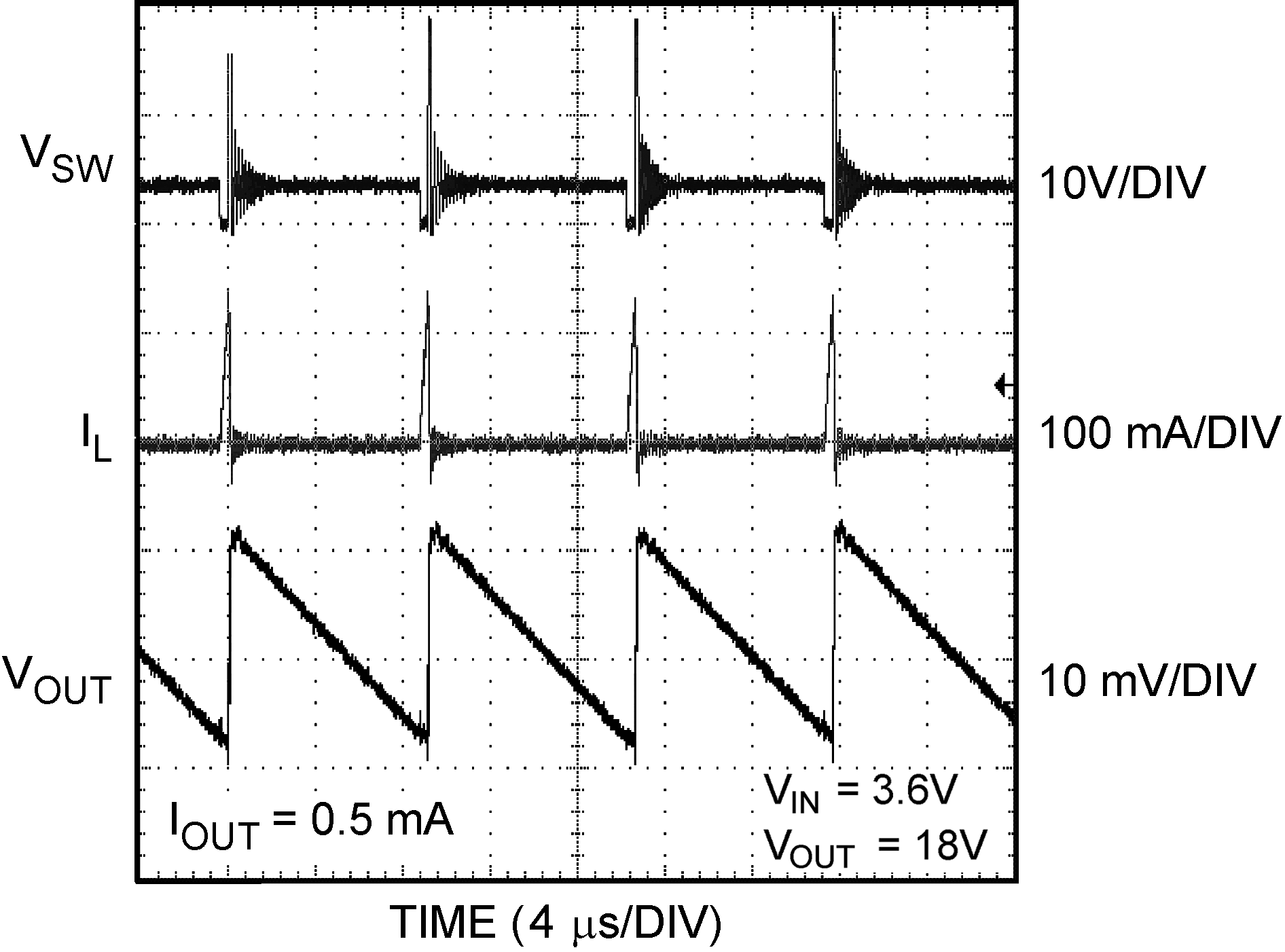
Copt, Ropt Included
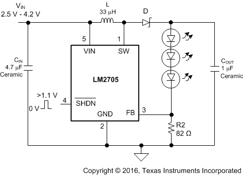
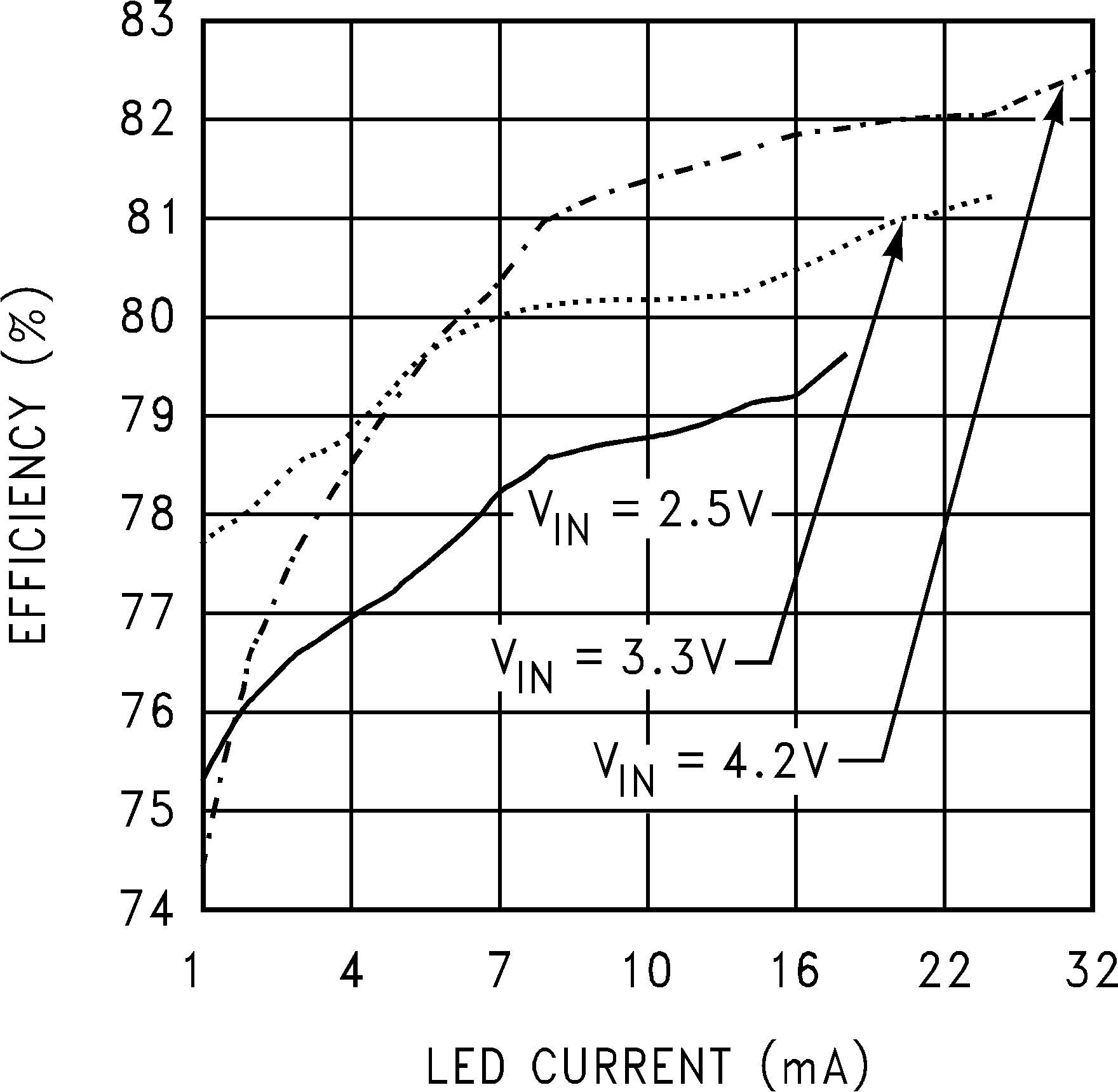 Figure 17. Two White-LED Efficiency
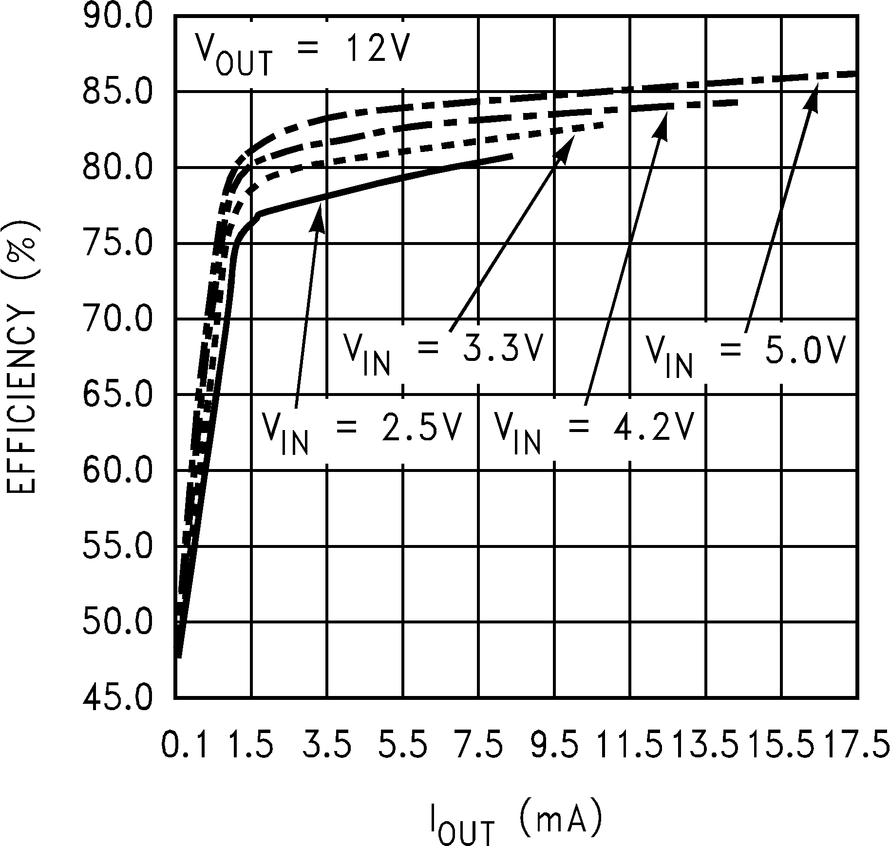
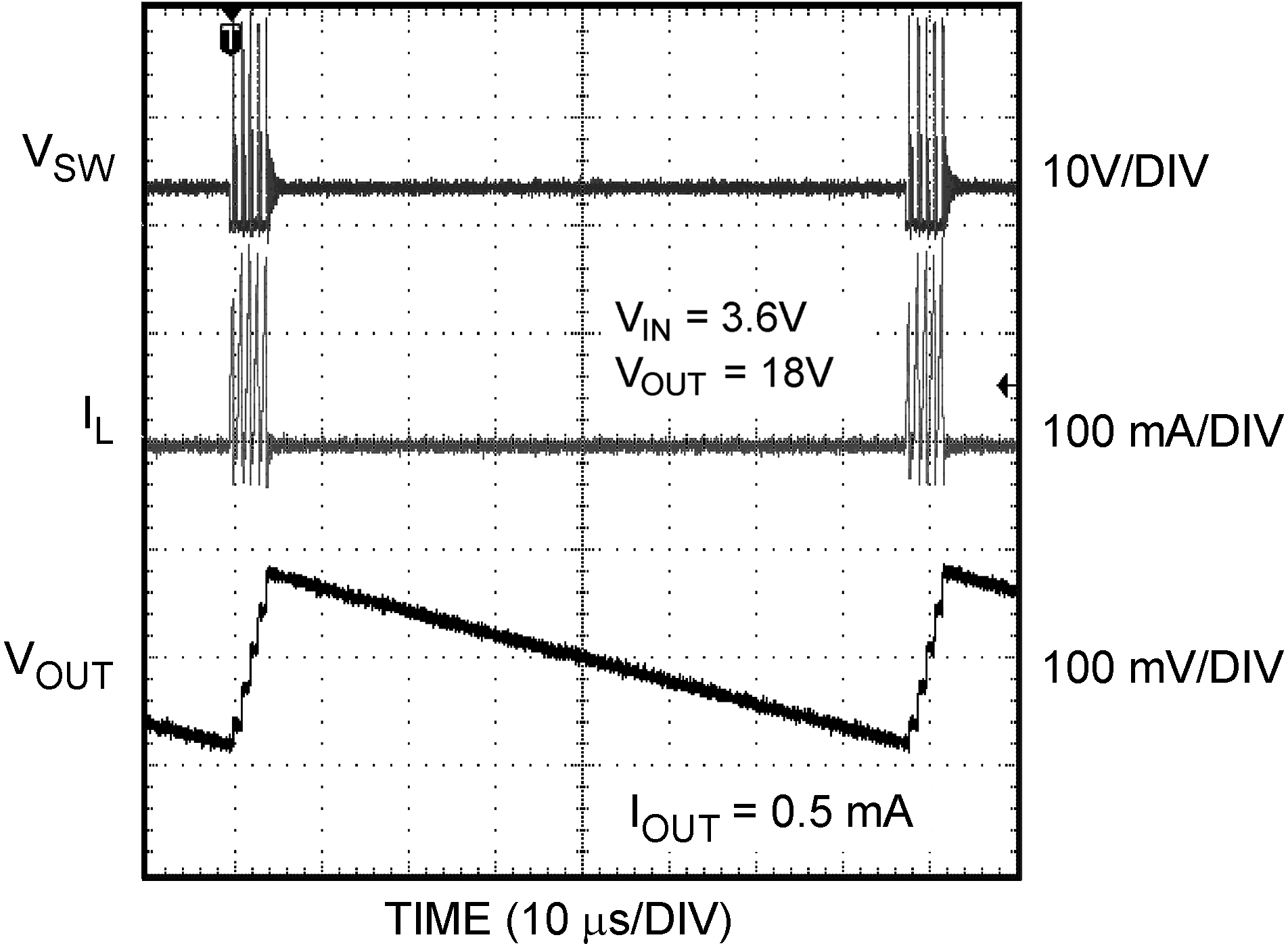
Copt, Ropt Excluded
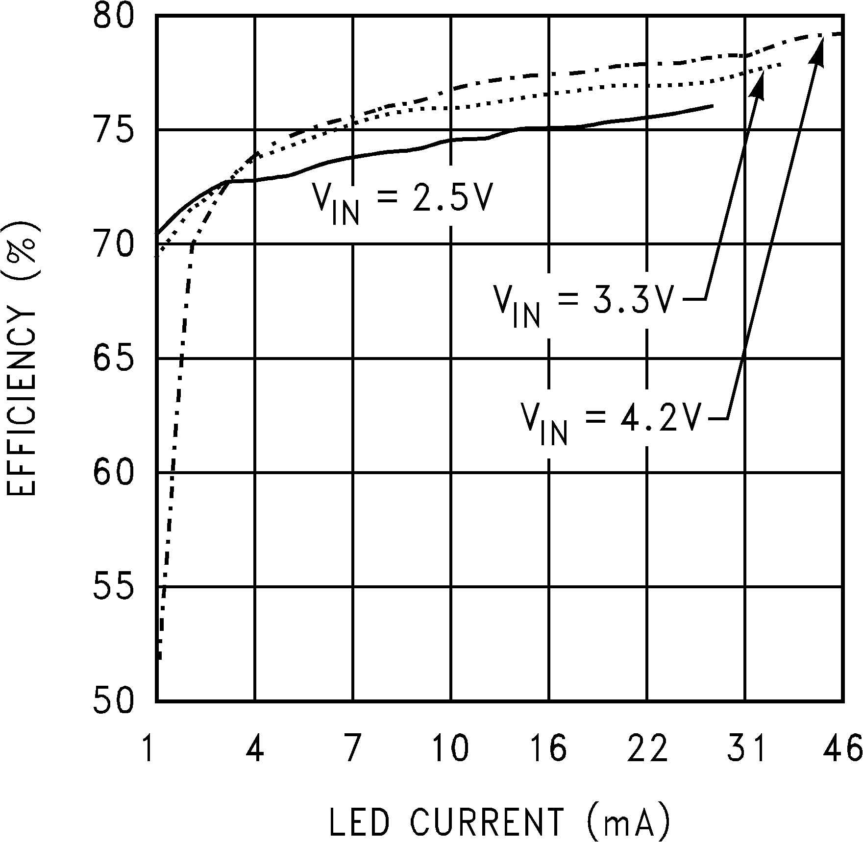 Figure 18. Three White-LED Efficiency
