ZHCSRY0M april 2000 – may 2023 LM2676
PRODUCTION DATA
- 1
- 1 特性
- 2 应用
- 3 说明
- 4 Revision History
- 5 Pin Configuration and Functions
-
6 Specifications
- 6.1 Absolute Maximum Ratings
- 6.2 ESD Ratings
- 6.3 Recommended Operating Conditions
- 6.4 Thermal Information
- 6.5 Electrical Characteristics: LM2676 – 3.3 V
- 6.6 Electrical Characteristics: LM2676 – 5 V
- 6.7 Electrical Characteristics: LM2676 – 12 B
- 6.8 Electrical Characteristics: LM2676 – Adjustable
- 6.9 Electrical Characteristics – All Output Voltage Versions
- 6.10 Typical Characteristics
- 7 Detailed Description
- 8 Application and Implementation
- 9 Device and Documentation Support
- 10Mechanical, Packaging, and Orderable Information
封装选项
机械数据 (封装 | 引脚)
散热焊盘机械数据 (封装 | 引脚)
- KTW|7
订购信息
8.2.4.2 Detailed Design Procedure
In this example, it is desired to convert the voltage from a two battery automotive power supply (voltage range of 20 V to 28 V, typical in large truck applications) to the 14.8-VDC alternator supply typically used to power electronic equipment from single battery 12-V vehicle systems. The load current required is 2 A (maximum). It is also desired to implement the power supply with all surface mount components.
Step 1: Operating conditions are:
- VOUT = 14.8 V
- VIN max = 28 V
- ILOAD max = 2 A
Step 2: Select an LM2676S-ADJ. To set the output voltage to 14.9 V, two resistors must be chosen (R1 and R2 in Figure 8-7). For the adjustable device, the output voltage is set by the following relationship:
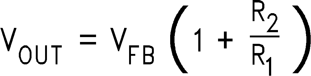
where
- VFB is the feedback voltage of typically 1.21 V
A recommended value to use for R1 is 1 kΩ. In this example, R2 is determined to be:
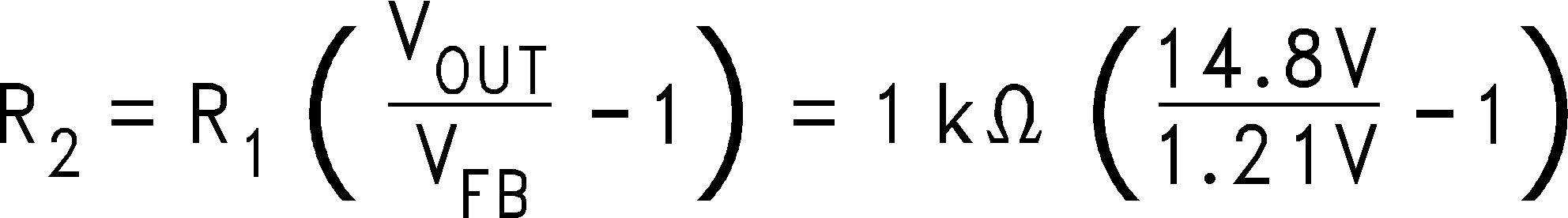
R2 = 11.23 kΩ
The closest standard 1% tolerance value to use is 11.3 kΩ.
This sets the nominal output voltage to 14.88 V which is within 0.5% of the target value.
Step 3: Using the nomograph for the adjustable device (Figure 8-5) requires a calculation of the inductor Volt × microsecond constant (E × T expressed in V × µS) from Equation 3:

where
- VSAT is the voltage drop across the internal power switch which is Rds(ON) × ILOAD
In this example, this is typically 0.15 Ω × 2 A or 0.3 V and VD is the voltage drop across the forward biased Schottky diode, typically 0.5 V. The switching frequency of 260 kHz is the nominal value to use to estimate the ON time of the switch during which energy is stored in the inductor.
For this example E × T is found to be:


Using Figure 8-5, the intersection of 27 V × µS horizontally and the 2 A vertical line (Iload max) indicates that L38, a 68-µH inductor, must be used.
From Table 8-3, L38 in a surface mount component is available from Pulse Engineering with part number PE-54038S.
Step 4: Use Table 8-9 or Table 8-10 to determine an output capacitor. With a 14.8-V output, the 12.5 to 15 V row is used, and with a 68-µH inductor, there are three surface mount output capacitor solutions. Table 8-1 or Table 8-2 provide the actual capacitor characteristics based on the C Code number. Any of the following choices can be used:
- 1 × 33-µF, 20 V AVX TPS (code C6)
- 1 × 47-µF, 20 V Sprague 594 (code C8)
- 1 / 47-µF, 20 V Kemet T495 (code C8)
When using the adjustable device in low voltage applications (less than 3-V output), if the nomograph (Figure 8-5) selects an inductance of 22 µH or less, Table 8-9 and Table 8-10 do not provide an output capacitor solution. With these conditions, the number of output capacitors required for stable operation becomes impractical. TI recommends to use either a 33-µH or 47-µH inductor and the output capacitors from Table 8-9 or Table 8-10.
Step 5: An input capacitor for this example requires at least a 35-V WV rating with an RMS current rating of 1 A (1/2 IOUT max). From Table 8-1 or Table 8-2, it can be seen that C12, a 33-µF, 35-V capacitor from Sprague, has the required voltage and current rating of the surface mount components.
Step 6: From Table 8-4, a 3-A Schottky diode must be selected. For surface mount diodes with a margin of safety on the voltage rating one of five diodes can be used:
- SK34
- 30BQ040
- 30WQ04F
- MBRS340
- MBRD340
Step 7: A 0.01-µF capacitor is used for CBOOST.