ZHCSGG7 June 2017 LM25118-Q1
PRODUCTION DATA.
- 1 特性
- 2 应用
- 3 说明
- 4 修订历史记录
- 5 Pin Configuration and Functions
- 6 Specifications
- 7 Detailed Description
-
8 Application and Implementation
- 8.1 Application Information
- 8.2
Typical Application
- 8.2.1 Design Requirements
- 8.2.2
Detailed Design Procedure
- 8.2.2.1 Custom Design With WEBENCH® Tools
- 8.2.2.2 R7 = RT
- 8.2.2.3 Inductor Selection - L1
- 8.2.2.4 R13 = RSENSE
- 8.2.2.5 C15 = CRAMP
- 8.2.2.6 Inductor Current Limit Calculation
- 8.2.2.7 C9 - C12 = Output Capacitors
- 8.2.2.8 D1
- 8.2.2.9 D4
- 8.2.2.10 C1 - C5 = Input Capacitors
- 8.2.2.11 C20
- 8.2.2.12 C8
- 8.2.2.13 C16 = CSS
- 8.2.2.14 R8, R9
- 8.2.2.15 R1, R3, C21
- 8.2.2.16 R2
- 8.2.2.17 Snubber
- 8.2.2.18 Error Amplifier Configuration
- 8.2.3 Application Curves
- 9 Power Supply Recommendations
- 10Layout
- 11器件和文档支持
- 12机械、封装和可订购信息
8 Application and Implementation
NOTE
Information in the following applications sections is not part of the TI component specification, and TI does not warrant its accuracy or completeness. TI’s customers are responsible for determining suitability of components for their purposes. Customers should validate and test their design implementation to confirm system functionality.
8.1 Application Information
The LM25118-Q1 high voltage switching regulator features all of the functions necessary to implement an efficient high voltage buck or buck-boost regulator using a minimum of external components. A buckboost regulator can maintain regulation for input voltages either higher or lower than the output voltage.
8.2 Typical Application
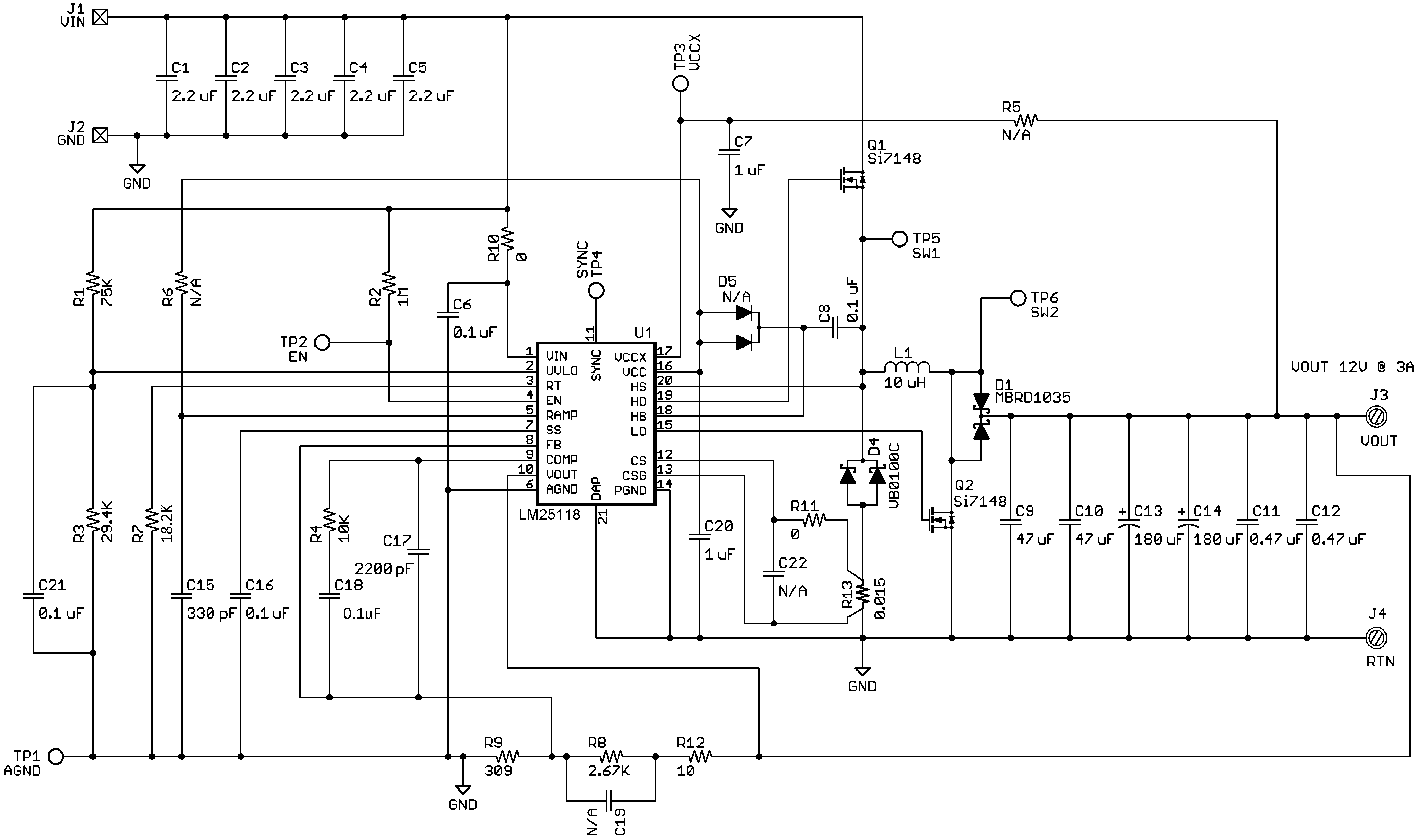
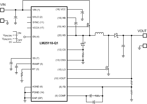 Figure 18. Typical Application Circuit
8.2.1 Design Requirements
The procedure for calculating the external components is illustrated with the following design example. The designations used in the design example correlate to the Figure 19. The design specifications are:
8.2.2 Detailed Design Procedure
8.2.2.1 Custom Design With WEBENCH® Tools
Click here to create a custom design using the LM25118-Q1 device with the WEBENCH® Power Designer.
- Start by entering the input voltage (VIN), output voltage (VOUT), and output current (IOUT) requirements.
- Optimize the design for key parameters such as efficiency, footprint, and cost using the optimizer dial.
- Compare the generated design with other possible solutions from Texas Instruments.
The WEBENCH Power Designer provides a customized schematic along with a list of materials with real-time pricing and component availability.
In most cases, these actions are available:
- Run electrical simulations to see important waveforms and circuit performance
- Run thermal simulations to understand board thermal performance
- Export customized schematic and layout into popular CAD formats
- Print PDF reports for the design, and share the design with colleagues
Get more information about WEBENCH tools at www.ti.com/WEBENCH.
8.2.2.2 R7 = RT
RT sets the oscillator switching frequency. Generally speaking, higher operating frequency applications will use smaller components, but have higher switching losses. An operating frequency of 300 kHz was selected for this example as a reasonable compromise for both component size and efficiency. The value of RT can be calculated as:

therefore, R7 = 18.3 kΩ
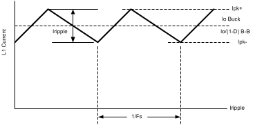 Figure 20. Inductor Current Waveform
8.2.2.3 Inductor Selection – L1
The inductor value is determined based upon the operating frequency, load current, ripple current, and the input and output voltages. See Figure 20 for details.
To keep the circuit in continuous conduction mode (CCM), the maximum ripple current IRIPPLE should be less than twice the minimum load current. For the specified minimum load of 0.6 A, the maximum ripple current is 1.2 Ap-p. Also, the minimum value of L must be calculated both for a buck and buck-boost configurations. The final value of inductance will generally be a compromise between the two modes. It is desirable to have a larger value inductor for buck mode, but the saturation current rating for the inductor must be large for buck-boost mode, resulting in a physically large inductor. Additionally, large value inductors present buck-boost mode loop compensation challenges which will be discussed in Error Amplifier Configuration . For the design example, the inductor values in both modes are calculated as:


where
- VOUT is the output voltage
- VIN(MAX) is the maximum input voltage
- f is the switching frequency
- IRIPPLE is the selected inductor peak to peak ripple current (1.2 A selected for this example)
- VIN(MIN) is the minimum input voltage
The resulting inductor values are:
A 10-µH inductor was selected which is a compromise between these values, while favoring the buck-boost mode. As illustrated in the compensation section, the inductor value should be as low as possible to move the buck-boost right-half-plane zero to a higher frequency. The ripple current is then rechecked with the selected inductor value using Equation 10 and Equation 11.
Because the inductor selected is lower than calculated for the Buck mode, the minimum load current for CCM in buck mode is 1.42 A at maximum VIN.
With a 10-µH inductor, the worst case peak inductor currents can be estimated for each case, assuming a 20% inductor value tolerance and 80% efficiency of the converter.
For this example, Equation 16 and Equation 17 yield:
An acceptable current limit setting would be 6.7 A for buck mode because the LM25118-Q1 automatically doubles the current limit threshold in buck-boost mode. The selected inductor must have a saturation current rating at least as high as the buck-boost mode cycle-by-cycle current limit threshold, in this case at least 13.5 A. A 10-µH, 15-A inductor was chosen for this application.
8.2.2.4 R13 = RSENSE
To select the current sense resistor, begin by calculating the minimum K values for each mode using Equation 20 and Equation 21. K represents the slope compensation of the controller and is different for each mode, KBUCK and KBUCK-BOOST. KBUCK and KBUCK-BOOST were selected to be 1.33 and 3, respectively.


Use Equation 24 and Equation 25 to calculate RSENSE for each mode of operation. A design margin, M, should be selected between 10%-30% to allow for component tolerances. For this design M was selected to be 10%.
An RSENSE value of no more than 15.5 mΩ must be used to ensure the required maximum output current in the buck-boost mode. A standard value of 15 mΩ was selected for this design.
8.2.2.5 C15 = CRAMP
With the inductor value selected, the value of C3 necessary for the emulation ramp circuit is:

With the inductance value (L1) selected as 10 µH, the calculated value for CRAMP is 333 pF. A standard value of 330 pF was selected.
8.2.2.6 Inductor Current Limit Calculation
The current limit for each mode can be calculated using Equation 29 and Equation 31. If the peak current limit is less than the calculated inductor peak current, the R13 and C15 need to be recalculated. This can be done by increasing the previous K values or M and reiterating the calculations.


8.2.2.7 C9 - C12 = Output Capacitors
In buck-boost mode, the output capacitors C9 – C12 must supply the entire output current during the switch on-time. For this reason, the output capacitors are chosen for operation in buck-boost mode, the demands being much less in buck operation. Both bulk capacitance and ESR must be considered to ensure a given output ripple voltage. Buck-boost mode capacitance can be estimated from:

ESR requirements can be estimated from:

For our example, with a ΔVOUT (output ripple) of 50 mV:
If hold-up times are a consideration, the values of input and output capacitors must be increased appropriately. Note that it is usually advantageous to use multiple capacitors in parallel to achieve the ESR value required. Also, it is good practice to put a 0.1-µF to 0.47-µF ceramic capacitor directly on the output pins of the supply to reduce high-frequency noise. Ceramic capacitors have good ESR characteristics, and are a good choice for input and output capacitors. Note that the effective capacitance of ceramic capacitors decreases with DC bias. For larger bulk values of capacitance, a low-ESR electrolytic is usually used. However, electrolytic capacitors have poor tolerance, especially over temperature, and the selected value should be selected larger than the calculated value to allow for temperature variation. Allowing for component tolerances, the following values of Cout were chosen for this design example:
Two 180-µF Oscon electrolytic capacitors for bulk capacitance
Two 47-µF ceramic capacitors to reduce ESR
Two 0.47-µF ceramic capacitors to reduce spikes at the output
8.2.2.8 D1
Reverse recovery currents degrade performance and decrease efficiency. For these reasons, a Schottky diode of appropriate ratings should be used for D1. The voltage rating of the boost diode should be equal to VOUT plus some margin.
8.2.2.9 D4
A Schottky type recirculating diode is required for all LM25118-Q1 applications. The near ideal reverse recovery characteristics and low forward voltage drop are particularly important diode characteristics for high input voltage and low output voltage applications. The reverse recovery characteristic determines how long the current surge lasts each cycle when the buck switch is turned on. The reverse recovery characteristics of Schottky diodes minimize the peak instantaneous power in the buck switch during the turn-on transition. The reverse breakdown rating of the diode should be selected for the maximum VIN plus some safety margin.
The forward voltage drop has a significant impact on the conversion efficiency, especially for applications with a low output voltage. Rated current for diodes vary widely from various manufacturers. For the LM25118-Q1 this current is user selectable through the current sense resistor value. Assuming a worst-case, 0.6-V drop across the diode, the maximum diode power dissipation can be high. The diode should have a voltage rating of VIN and a current rating of IOUT. A conservative design would at least double the advertised diode rating because specifications between manufacturers vary. For the reference design, a 100-V, 10-A Schottky in a D2PAK package was selected.
8.2.2.10 C1 – C5 = Input Capacitors
A typical regulator supply voltage has a large source impedance at the switching frequency. Good-quality input capacitors are necessary to limit the ripple voltage at the VIN pin while supplying most of the switch current during the buck switch on-time. When the buck switch turns on, the current into the buck switch steps from zero to the lower peak of the inductor current waveform, then ramps up to the peak value, and then drops to the zero at turnoff. The RMS current rating of the input capacitors depends on which mode of operation is most critical.

The RMS current demand on the input capacitor(s) is at the maximum value when the duty cycle is at 50%.

Checking both modes of operation we find:
Therefore C1 — C5 should be sized to handle 4.7 A of ripple current. Quality ceramic capacitors with a low ESR should be selected. To allow for capacitor tolerances, five 2.2-µF, 100-V ceramic capacitors will be used. If step input voltage transients are expected near the maximum rating of the LM25118-Q1, a careful evaluation of the ringing and possible spikes at the device VIN pin should be completed. An additional damping network or input voltage clamp may be required in these cases.
8.2.2.11 C20
The capacitor at the VCC pin provides noise filtering and stability for the VCC regulator. The recommended value of C20 should be no smaller than 0.1 µF, and should be a good-quality, low-ESR, ceramic capacitor. A value of 1 µF was selected for this design. C20 should be 10 x C8.
If operating without VCCX, then
must be less than the VCC current limit.
8.2.2.12 C8
The bootstrap capacitor between the HB and HS pins supplies the gate current to charge the buck switch gate at turnon. The recommended value of C8 is 0.1 µF to 0.47 µF, and should be a good-quality, low-ESR, ceramic capacitor. A value of 0.1 µF was chosen for this design.
8.2.2.13 C16 = CSS
The capacitor at the SS pin determines the soft-start time, that is, the time for the reference voltage and the output voltage, to reach the final regulated value. The time is determined from:

and assumes a current limit>Iload + ICout
For this application, a C16 value of 0.1 µF was chosen which corresponds to a soft-start time of about 12 ms.
8.2.2.14 R8, R9
R8 and R9 set the output voltage level, the ratio of these resistors is calculated from:

For a 12-V output, the R8/R9 ratio calculates to 8.76. The resistors should be chosen from standard value resistors and a good starting point is to select resistors within power ratings appropriate for the output voltage. Values of 309 Ω for R9 and 2.67 kΩ for R8 were selected.
8.2.2.15 R1, R3, C21
A voltage divider can be connected to the UVLO pin to set a minimum operating voltage VIN(UVLO) for the regulator. If this feature is required, the easiest approach to select the divider resistor values is to choose a value for R1 between 10 kΩ and 100 kΩ, while observing the minimum value of R1 necessary to allow the UVLO switch to pull the UVLO pin low. This value is:
R1 ≥ 1000 × VIN(MAX)
R1 ≥ 75 k
R3 is then calculated from:

Because VIN(MIN) for our example is 5 V, set VIN(UVLO) to 4 V for some margin in component tolerances and input ripple.
R1 = 75 k is chosen because it is a standard value
R3 = 29.332 k is calculated from Equation 44. 29.4 k was used because it is a standard value
Capacitor C21 provides filtering for the divider and the off time of the hiccup duty cycle during current limit. The voltage at the UVLO pin should never exceed 15 V when using an external set-point divider. It may be necessary to clamp the UVLO pin at high input voltages.
Knowing the desired off time during hiccup current limit, the value of C21 is given by:
Notice that tOFF varies with VIN
In this example, C21 was chosen to be 0.1 µF. This will set the tOFF time to 723 µs with VIN = 12 V.
8.2.2.16 R2
A 1-M pullup resistor connected from the EN pin to the VIN pin is sufficient to keep enable in a high state if on-off control is not used.
8.2.2.17 Snubber
A snubber network across the buck recirculating diode reduces ringing and spikes at the switching node. Excessive ringing and spikes can cause erratic operation and increase noise at the regulator output. In the limit, spikes beyond the maximum voltage rating of the LM25118-Q1 or the recirculating diode can damage these devices. Selecting the values for the snubber is best accomplished through empirical methods. First, make sure the lead lengths for the snubber connections are very short. Start with a resistor value between 5 and 20 Ω. Increasing the value of the snubber capacitor results in more damping, however the snubber losses increase. Select a minimum value of the capacitor that provides adequate clamping of the diode waveform at maximum load. A snubber may be required for the boost diode as well. The same empirical procedure applies. Snubbers were not necessary in this example.
8.2.2.18 Error Amplifier Configuration
8.2.2.18.1 R4, C18, C17
These components configure the error amplifier gain characteristics to accomplish a stable overall loop gain. One advantage of current mode control is the ability to close the loop with only three feedback components, R4, C18, and C17. The overall loop gain is the product of the modulator gain and the error amplifier gain. The DC modulator gain of the LM25118-Q1 is as follows:

The dominant, low frequency pole of the modulator is determined by the load resistance (RLOAD) and output capacitance (COUT). The corner frequency of this pole is:

For this example, RLOAD = 4 Ω, DMAX = 0.705, and COUT = 454 µF, therefore:
Additionally, there is a right-half plane (RHP) zero associated with the modulator. The frequency of the RHP zero is:

The output capacitor ESR produces a zero given by:

The RHP zero complicates compensation. The best design approach is to reduce the loop gain to cross zero at about 25% of the calculated RHP zero frequency. The Type ll error amplifier compensation provided by R4, C18, and C17 places one pole at the origin for high DC gain. The second pole should be placed close to the RHP zero. The error amplifier zero (Equation 54) should be placed near the dominate modulator pole. This is a good starting point for compensation.
Components R4 and C18 configure the error amplifier as a Type II configuration which has a DC pole and a zero at

C17 introduces an additional pole used to cancel high frequency switching noise. The error amplifier zero cancels the modulator pole leaving a single pose response at the crossover frequency of the loop gain if the crossover frequency is much lower than the right half plane zero frequency. A single pole response at the crossover frequency yields a very stable loop with 90 degrees of phase margin.
For the design example, a target loop bandwidth (crossover frequency) of 2.0 kHz was selected (about 25% of the right-half-plane zero frequency). The error amplifier zero (fz) should be selected at a frequency near that of the modulator pole and much less than the target crossover frequency. This constrains the product of R4 and C18 for a desired compensation network zero to be less than 2 kHz. Increasing R4, while proportionally decreasing C18 increases the error amp gain. Conversely, decreasing R4 while proportionally increasing C18 decreases the error amp gain. For the design example C18 was selected for 100 nF and R4 was selected to be 10 kΩ. These values set the compensation network zero at 159 Hz. The overall loop gain can be predicted as the sum (in dB) of the modulator gain and the error amp gain.
If a network analyzer is available, the modulator gain can be measured and the error amplifier gain can be configured for the desired loop transfer function. If a network analyzer is not available, the error amplifier compensation components can be designed with the guidelines given. Step load transient tests can be performed to verify acceptable performance. The step load goal is minimal overshoot with a damped response.
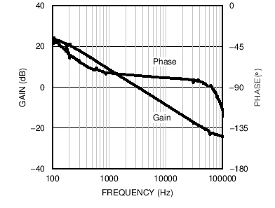
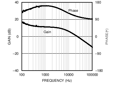
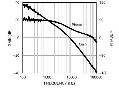
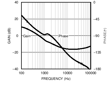
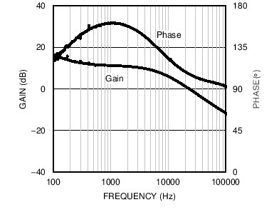
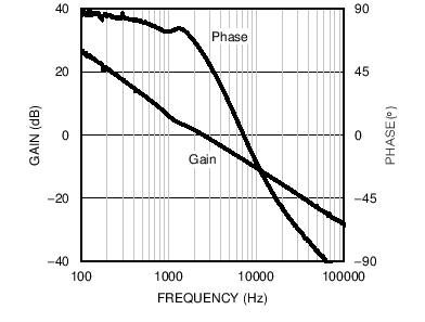
Please see the plots shown in Figure 21 through Figure 26 which illustrate the gain and phase diagrams of the design example.
8.2.3 Application Curves
The plots shown in Figure 21 through Figure 26 show the gain and phase diagrams of the design example. The overall bandwidth is lower in a buck-boost application due the compensation challenges associated with the right-half-plane zero. For a pure buck application, the bandwidth could be much higher. The LM5116 data sheet is a good reference for compensation design of a pure buck mode regulator.
