ZHCS538M September   2008  – October 2020 LM22678 , LM22678-Q1

PRODUCTION DATA  

  1. 特性
  2. 应用
  3. 说明
  4. Revision History
  5. Pin Configuration and Functions
  6. Specifications
    1. 6.1 Absolute Maximum Ratings
    2. 6.2 Handling Ratings: LM22678
    3. 6.3 Handling Ratings: LM22678-Q1
    4. 6.4 Recommended Operating Conditions
    5. 6.5 Thermal Information
    6. 6.6 Electrical Characteristics
    7. 6.7 Typical Characteristics
  7. Detailed Description
    1. 7.1 Overview
    2. 7.2 Functional Block Diagram
    3. 7.3 Feature Description
      1. 7.3.1 Precision Enable and UVLO
      2. 7.3.2 Soft Start
      3. 7.3.3 Bootstrap Supply
      4. 7.3.4 Internal Loop Compensation
    4. 7.4 Device Functional Modes
      1. 7.4.1 Shutdown Mode
      2. 7.4.2 Active Mode
      3. 7.4.3 Current Limit
      4. 7.4.4 Thermal Protection
      5. 7.4.5 Duty-Cycle Limits
  8. Application and Implementation
    1. 8.1 Application Information
      1. 8.1.1 Output Voltage Divider Selection
      2. 8.1.2 Power Diode
    2. 8.2 Typical Applications
      1. 8.2.1 Typical Buck Regulator Application
        1. 8.2.1.1 Design Requirements
        2. 8.2.1.2 Detailed Design Procedure
          1. 8.2.1.2.1 External Components
            1. 8.2.1.2.1.1 Inductor
          2. 8.2.1.2.2 Input Capacitor
          3. 8.2.1.2.3 Output Capacitor
          4. 8.2.1.2.4 Bootstrap Capacitor
        3. 8.2.1.3 Application Curves
  9. Layout
    1. 9.1 Layout Guidelines
    2. 9.2 Layout Example
    3. 9.3 Thermal Considerations
  10. 10Device and Documentation Support
    1. 10.1 Documentation Support
      1. 10.1.1 Related Documentation
    2. 10.2 支持资源
    3. 10.3 接收文档更新通知
    4. 10.4 静电放电警告
    5. 10.5 术语表

封装选项

机械数据 (封装 | 引脚)
散热焊盘机械数据 (封装 | 引脚)
订购信息

Pin Configuration and Functions

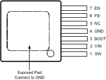
GUID-50AB474F-339B-4E17-B87A-E07503806E2F-low.gif Figure 5-1 7-Pin PFM Package (Top View)
Table 5-1 Pin Functions
PIN TYPE DESCRIPTION APPLICATION INFORMATION
NAME NO.
BOOT 3 I Bootstrap input Provides the gate voltage for the high-side NFET.
EN 7 I Enable input Used to control regulator start-up and shutdown. See Section 7.3.1.
EP EP Exposed pad Connect to ground. Provides thermal connection to PCB. See Section 8.
FB 6 I Feedback input Feedback input to the regulator
GND 4 Ground input to regulator;
system common
System ground pin
NC 5 Not connected Pin is not electrically connected inside chip. Pin does function as thermal conductor.
SW 1 O Switch pin Switching output of regulator
VIN 2 I Input voltage Supply input to the regulator