ZHCS538M September 2008 – October 2020 LM22678 , LM22678-Q1
PRODUCTION DATA
- 1 特性
- 2 应用
- 3 说明
- 4 Revision History
- 5 Pin Configuration and Functions
- 6 Specifications
- 7 Detailed Description
- 8 Application and Implementation
- 9 Layout
- 10Device and Documentation Support
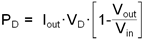
9.3 Thermal Considerations
The components with the highest power dissipation are the power diode and the power MOSFET internal to the LM22678 regulator. The easiest method to determine the power dissipation within the LM22678 is to measure the total conversion losses then subtract the power losses in the diode and inductor. The total conversion loss is the difference between the input power and the output power. An approximation for the power diode loss is shown in Equation 17.
where
- VD is the diode voltage drop.
An approximation for the inductor power is determined by Equation 18.

where
- RL is the dc resistance of the inductor.
The 1.1 factor is an approximation for the ac losses.
The regulator has an exposed thermal pad to aid power dissipation. Adding multiple vias under the device to the ground plane will greatly reduce the regulator junction temperature. Selecting a diode with an exposed pad will also aid the power dissipation of the diode. The most significant variables that affect the power dissipation of the regulator are output current, input voltage and operating frequency. The power dissipated while operating near the maximum output current and maximum input voltage can be appreciable. The junction-to-ambient thermal resistance of the LM22678 will vary with the application. The most significant variables are the area of copper in the PC board, the number of vias under the IC exposed pad and the amount of forced air cooling provided. A large continuous ground plane on the top or bottom PCB layer will provide the most effective heat dissipation. The integrity of the solder connection from the IC exposed pad to the PC board is critical. Excessive voids will greatly diminish the thermal dissipation capacity. The junction-to-ambient thermal resistance of the LM22678 PFM package is specified in Section 6.6. See AN-2020 Thermal Design By Insight, Not Hindsight (SNVA419) for more information.