SWRS283A June   2022  – November 2022 IWR6243

PRODUCTION DATA  

  1. Features
  2. Applications
  3. Description
  4. Functional Block Diagram
  5. Revision History
  6. Device Comparison
    1. 6.1 Related Products
  7. Terminal Configuration and Functions
    1. 7.1 Pin Diagram
    2. 7.2 Signal Descriptions
  8. Specifications
    1. 8.1 Absolute Maximum Ratings
    2. 8.2 ESD Ratings
    3. 8.3 Power-On Hours (POH)
    4. 8.4 Recommended Operating Conditions
    5. 8.5 Power Supply Specifications
    6. 8.6 Power Consumption Summary
    7. 8.7 RF Specification
    8. 8.8 Thermal Resistance Characteristics for FCBGA Package [ABL0161]
    9. 8.9 Timing and Switching Characteristics
      1. 8.9.1 Power Supply Sequencing and Reset Timing
      2. 8.9.2 Synchronized Frame Triggering
      3. 8.9.3 Input Clocks and Oscillators
        1. 8.9.3.1 Clock Specifications
      4. 8.9.4 Multibuffered / Standard Serial Peripheral Interface (MibSPI)
        1. 8.9.4.1 Peripheral Description
          1. 8.9.4.1.1 SPI Timing Conditions
          2. 8.9.4.1.2 SPI Peripheral Mode Switching Parameters (SPICLK = input, SPISIMO = input, and SPISOMI = output)
          3. 8.9.4.1.3 SPI Peripheral Mode Timing Requirements (SPICLK = input, SPISIMO = input, and SPISOMI = output)
        2. 8.9.4.2 Typical Interface Protocol Diagram (Peripheral Mode)
      5. 8.9.5 Inter-Integrated Circuit Interface (I2C)
        1. 8.9.5.1 I2C Timing Requirements
      6. 8.9.6 LVDS Interface Configuration
        1. 8.9.6.1 LVDS Interface Timings
      7. 8.9.7 General-Purpose Input/Output
        1. 8.9.7.1 Switching Characteristics for Output Timing versus Load Capacitance (CL)
      8. 8.9.8 Camera Serial Interface (CSI2)
        1. 8.9.8.1 CSI2 Switching Characteristics
  9. Detailed Description
    1. 9.1 Overview
    2. 9.2 Functional Block Diagram
    3. 9.3 Subsystems
      1. 9.3.1 RF and Analog Subsystem
        1. 9.3.1.1 Clock Subsystem
        2. 9.3.1.2 Transmit Subsystem
        3. 9.3.1.3 Receive Subsystem
      2. 9.3.2 Host Interface
    4. 9.4 Other Subsystems
      1. 9.4.1 ADC Data Format Over CSI2 Interface
      2. 9.4.2 ADC Channels (Service) for User Application
        1. 9.4.2.1 GPADC Parameters
  10. 10Monitoring and Diagnostic Mechanisms
  11. 11Applications, Implementation, and Layout
    1. 11.1 Application Information
    2. 11.2 Radar Sensor for Industrial Applications
    3. 11.3 Imaging Radar using Cascade Configuration
  12. 12Device and Documentation Support
    1. 12.1 Device Nomenclature
    2. 12.2 Documentation Support
    3. 12.3 Support Resources
    4. 12.4 Trademarks
    5. 12.5 Electrostatic Discharge Caution
    6. 12.6 Export Control Notice
    7. 12.7 Glossary
  13. 13Mechanical, Packaging, and Orderable Information
    1. 13.1 Packaging Information
    2.     Package Option Addendum
    3. 13.2 Tape and Reel Information
    4.     Tray Information
    5.     Mechanical Data

封装选项

请参考 PDF 数据表获取器件具体的封装图。

机械数据 (封装 | 引脚)
  • ABL|161
散热焊盘机械数据 (封装 | 引脚)
订购信息

Transmit Subsystem

The IWR6243 device transmit subsystem consists of three parallel transmit chains, each with independent phase and amplitude control. All three transmitters can be used simultaneously or in time-multiplexed fashion. The IWR6243 device supports binary phase modulation for MIMO radar and interference mitigation.

GUID-5CC70217-35A7-4071-B082-58F4385EABCF.html specifies the maximum power each transmit chain can deliver, at the antenna port on the PCB. The transmit chains also support programmable backoff for system optimization and also to meet the local regulatory emission requirements.

#X6350 describes the transmit subsystem.
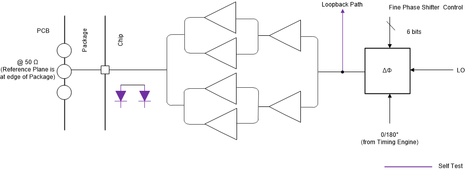
GUID-20210127-CA0I-ZHMG-QK1Q-KG05BFVHTK5V-low.gif Figure 9-2 Transmit Subsystem (Per Channel)