ZHCSDO5C April 2015 – September 2023
PRODUCTION DATA
- 1
- 1 特性
- 2 应用
- 3 说明
- 4 Revision History
- 5 Pin Configuration and Functions
- 6 Specifications
- 7 Detailed Description
- 8 Applications and Implementation
- 9 Device and Documentation Support
- 10Mechanical, Packaging, and Orderable Information
7.4.2.1 Calculating Gain Error Resulting from External Filter Resistance
If additional external series filter resistors are added to the circuit, the mismatch in bias currents results in a mismatch of voltage drops across the filter resistors. This mismatch creates a differential error voltage that subtracts from the voltage developed across the Kelvin connection of the shunt resistor, thus reducing the voltage that reaches the amplifier input terminals. Without the additional series resistance, the mismatch in input bias currents has little effect on device operation as a result of the low input bias current of the amplifier and the typically low impedance of the traces between the shunt and amplifier input pins. The amount of error these external filter resistors add to the measurement can be calculated using Equation 3, where the gain error factor is calculated using Equation 2.
The amount of variance between the differential voltage present at the device input relative to the voltage developed at the shunt resistor is based both on the external series resistance value as well as the internal input resistors, RINT; see Figure 7-4. The reduction of the shunt voltage reaching the device input pins appears as a gain error when comparing the output voltage relative to the voltage across the shunt resistor. A factor can be calculated to determine the amount of gain error that is introduced by the addition of external series resistance. Equation 2 calculates the expected deviation from the shunt voltage compared to the expected voltage at the device input pins.
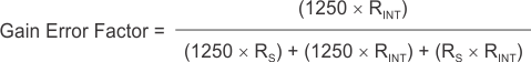
where:
- RINT is the internal input resistor and
- RS is the external series resistance

With the adjustment factor equation including the device internal input resistance, this factor varies with each gain version; see Table 7-1. Each individual device gain error factor is listed in Table 7-2.
The gain error that can be expected from the addition of the external series resistors can then be calculated based on Equation 3.
| DEVICE | GAIN | RINT |
|---|---|---|
| INA250A1 | 200 mV/A | 50 kΩ |
| INA250A2 | 500 mV/A | 20 kΩ |
| INA250A3 | 800 mV/A | 12.5 kΩ |
| INA250A4 | 2 V/A | 5 kΩ |
| DEVICE | SIMPLIFIED GAIN ERROR FACTOR |
|---|---|
| INA250A1 |  |
| INA250A2 |  |
| INA250A3 |  |
| INA250A4 |  |
For example, using an INA250A2 and the corresponding gain error equation from Table 7-2, a series resistance of 10 Ω results in a gain error factor of 0.991. The corresponding gain error is then calculated using Equation 3, resulting in a gain error of approximately 0.84% because of the external 10-Ω series resistors.