ZHCSTR6A September   1999  – November 2023 INA146

PRODUCTION DATA  

  1.   1
  2. 1特性
  3. 2应用
  4. 3说明
  5. 4Pin Configuration and Functions
  6. 5Specifications
    1. 5.1 Absolute Maximum Ratings
    2. 5.2 ESD Ratings
    3. 5.3 Recommended Operating Conditions
    4. 5.4 Thermal Information
    5. 5.5 Electrical Characteristics VS = ±2.25 V to ±18 V
    6. 5.6 Electrical Characteristics VS = 5 V Single Supply
    7. 5.7 Amplifier A1, A2 Performance
    8. 5.8 Typical Performance Curves
  7. 6Application and Implementation
    1. 6.1 Application Information
      1. 6.1.1 Operating Voltage
      2. 6.1.2 Setting the Gain
      3. 6.1.3 Common-mode Range
      4. 6.1.4 Offset Trim
      5. 6.1.5 Input Impedance
  8. 7Device and Documentation Support
    1. 7.1 第三方产品免责声明
    2. 7.2 Documentation Support
      1. 7.2.1 Related Documentation
    3. 7.3 接收文档更新通知
    4. 7.4 支持资源
    5. 7.5 Trademarks
    6. 7.6 静电放电警告
    7. 7.7 术语表
  9. 8Revision History
  10. 9Mechanical, Packaging, and Orderable Information

封装选项

请参考 PDF 数据表获取器件具体的封装图。

机械数据 (封装 | 引脚)
  • D|8
散热焊盘机械数据 (封装 | 引脚)
订购信息

Common-mode Range

The 10:1 input resistor ratio of the INA146 provides an input common-mode range that can extend well beyond the power supply rails. Exact range depends on the power supply voltage and the voltage applied to the Ref terminal (pin 1). For proper operation, the voltage at the non-inverting input of A1 (an internal node) must be within the linear operating range. The voltage is determined by the simple 10:1 voltage divider between pin 3 and pin 1. This voltage must be between V– and (V+) – 1 V.
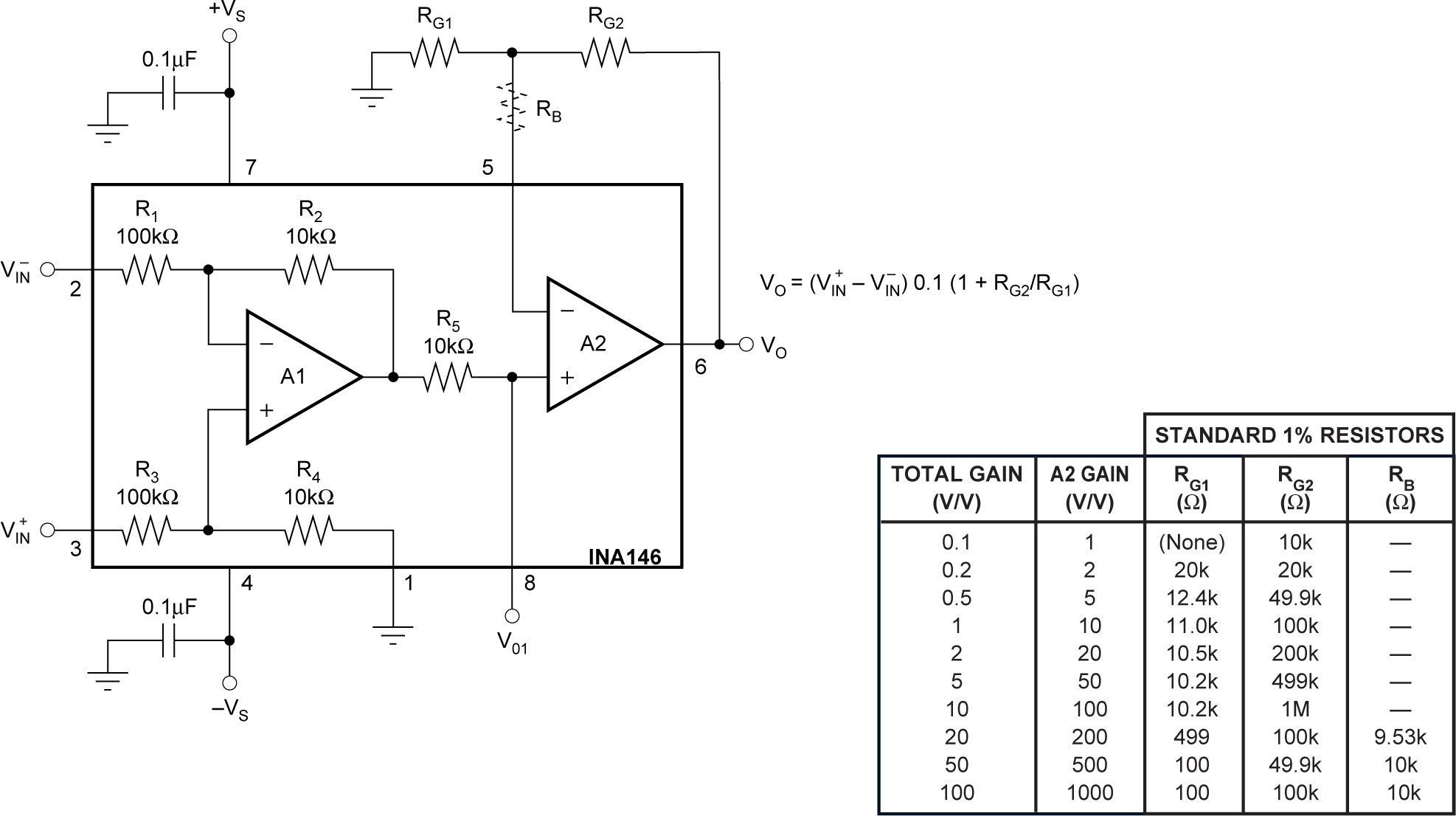
GUID-6B0A2B6E-6394-4BA8-9316-02AFF3EC06FA-low.png Figure 6-1 Basic Circuit Connections