ZHCSFO0J September 2003 – August 2018 INA138-Q1 , INA168-Q1
PRODUCTION DATA.
- 1 特性
- 2 应用
- 3 说明
- 4 修订历史记录
- 5 Pin Configuration and Functions
- 6 Specifications
- 7 Detailed Description
-
8 Application and Implementation
- 8.1 Application Information
- 8.2 Typical Applications
- 9 Power Supply Recommendations
- 10Layout
- 11器件和文档支持
- 12机械、封装和可订购信息
8.1.1 Operation
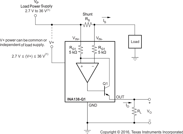
Figure 9 illustrates the basic circuit diagram for both the INA138-Q1 and INA168-Q1. Load current IS is drawn from supply VP through shunt resistor RS. The voltage drop in the shunt resistor is forced across RG1 by the internal op amp, causing current to flow into the collector of Q1. External resistor RL converts the output current, IO, to a voltage, VOUT, at the OUT pin. The transfer function for the INA1x8-Q1 is shown in Equation 3:
where
- gm = 200 μA/V
In the circuit of Figure 9, the input voltage, (VIN+ − VIN−), is equal to IS × RS. The output voltage, VOUT, is equal to IO × RL. The transconductance, gm, of the INA1x8-Q1 is 200 μA/V. The complete transfer function for the current measurement amplifier in this application is shown in Equation 4:
The maximum differential input voltage for accurate measurements is 0.5 V, producing a 100-μA output current. A differential input voltage of up to 2 V does not cause damage. Differential measurements (VIN+ and VIN− pins) must be unipolar, with a more-positive voltage applied to the VIN+ pin. If a more-negative voltage is applied to the VIN+ pin, IO goes to zero, but no damage occurs.
Table 1. Voltage Gains and Corresponding Load-Resistor Values
| VOLTAGE GAIN | EXACT RL (kΩ) | NEAREST 1% RL (kΩ) |
|---|---|---|
| 1 | 5 | 4.99 |
| 2 | 10 | 10 |
| 5 | 25 | 24.9 |
| 10 | 50 | 49.9 |
| 20 | 100 | 100 |
| 50 | 250 | 249 |
| 100 | 500 | 499 |
