ZHCSW26B September 2000 – April 2024 INA117
PRODUCTION DATA
- 1
- 1 特性
- 2 应用
- 3 说明
- 4 Pin Configuration and Functions
- 5 Specifications
- 6 Typical Characteristics
- 7 Application and Implementation
- 8 Device and Documentation Support
- 9 Revision History
- 10Mechanical, Packaging, and Orderable Information
封装选项
请参考 PDF 数据表获取器件具体的封装图。
机械数据 (封装 | 引脚)
- D|8
- P|8
- LMC|8
散热焊盘机械数据 (封装 | 引脚)
订购信息
7.1.2 Transfer Function
Most applications use the INA117 as a simple unity-gain difference amplifier. The transfer function is:
V0 = V3 – V2V3 and V2 are the voltages at pins 3 and 2.
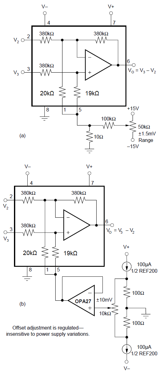
 Figure 7-2 Offset Voltage Trim
Circuits
Figure 7-2 Offset Voltage Trim
CircuitsSome applications, however, apply voltages to the reference terminals (pins 1 and 5). A more complete transfer function is:
V0 = V3 – V2 + 19 × V5 – 18 × V1V5 and V1 are the voltages at pins 5 and 1.