ZHCSTC7A September 2000 – January 2024 INA114
PRODUCTION DATA
- 1
- 1 特性
- 2 应用
- 3 说明
- 4 Pin Configuration and Functions
- 5 Specifications
- 6 Application and Implementation
- 7 Typical Applications
- 8 Device and Documentation Support
- 9 Revision History
- 10Mechanical, Packaging, and Orderable Information
封装选项
请参考 PDF 数据表获取器件具体的封装图。
机械数据 (封装 | 引脚)
- P|8
- DW|16
散热焊盘机械数据 (封装 | 引脚)
订购信息
6.1 Application Information
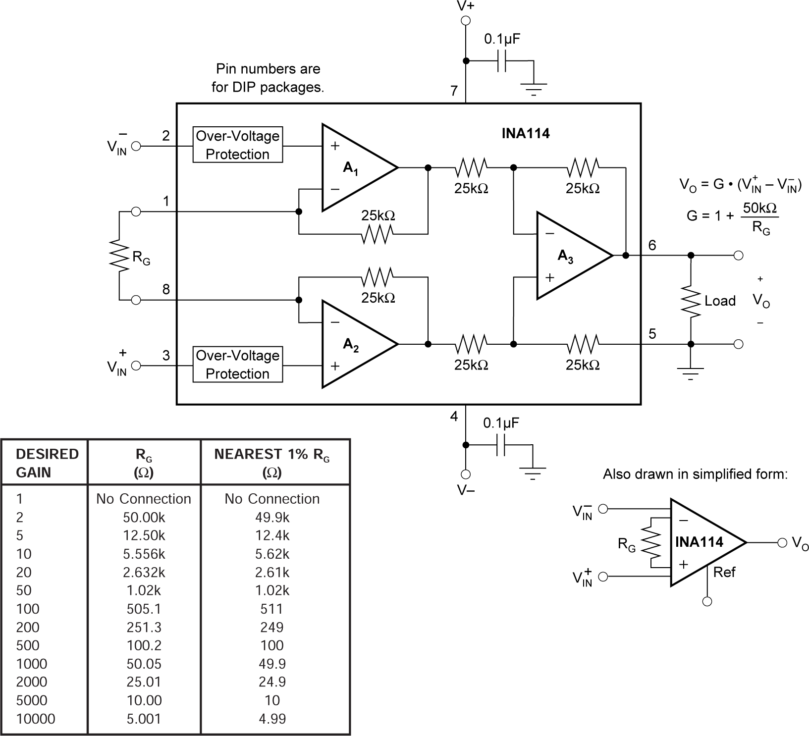
Figure 6-1 shows the basic connections required for operation of the INA114. Applications with noisy or high-impedance power supplies can require decoupling capacitors close to the device pins as shown.
 Figure 6-1 Basic Connections.
The output is referred to the output reference (Ref) pin, which is normally grounded. This connection must be low-impedance to provide good common-mode rejection. A resistance of 5Ω in series with the Ref pin causes a typical device to degrade to approximately 80dB CMR (G = 1).