ZHCSF09 May 2016 FDC2112-Q1 , FDC2114-Q1 , FDC2212-Q1 , FDC2214-Q1
PRODUCTION DATA.
- 1 特性
- 2 应用
- 3 说明
- 4 修订历史记录
- 5 Pin Configuration and Functions
- 6 Specifications
-
7 Detailed Description
- 7.1 Overview
- 7.2 Functional Block Diagrams
- 7.3 Feature Description
- 7.4 Device Functional Modes
- 7.5 Programming
- 7.6
Register Maps
- 7.6.1 Register List
- 7.6.2 Address 0x00, DATA_CH0
- 7.6.3 Address 0x01, DATA_LSB_CH0 (FDC2212 / FDC2214 only)
- 7.6.4 Address 0x02, DATA_CH1
- 7.6.5 Address 0x03, DATA_LSB_CH1 (FDC2212 / FDC2214 only)
- 7.6.6 Address 0x04, DATA_CH2 (FDC2114, FDC2214 only)
- 7.6.7 Address 0x05, DATA_LSB_CH2 (FDC2214 only)
- 7.6.8 Address 0x06, DATA_CH3 (FDC2114, FDC2214 only)
- 7.6.9 Address 0x07, DATA_LSB_CH3 (FDC2214 only)
- 7.6.10 Address 0x08, RCOUNT_CH0
- 7.6.11 Address 0x09, RCOUNT_CH1
- 7.6.12 Address 0x0A, RCOUNT_CH2 (FDC2114, FDC2214 only)
- 7.6.13 Address 0x0B, RCOUNT_CH3 (FDC2114, FDC2214 only)
- 7.6.14 Address 0x0C, OFFSET_CH0 (FDC21112 / FDC2114 only)
- 7.6.15 Address 0x0D, OFFSET_CH1 (FDC21112 / FDC2114 only)
- 7.6.16 Address 0x0E, OFFSET_CH2 (FDC2114 only)
- 7.6.17 Address 0x0F, OFFSET_CH3 (FDC2114 only)
- 7.6.18 Address 0x10, SETTLECOUNT_CH0
- 7.6.19 Address 0x11, SETTLECOUNT_CH1
- 7.6.20 Address 0x12, SETTLECOUNT_CH2 (FDC2114, FDC2214 only)
- 7.6.21 Address 0x13, SETTLECOUNT_CH3 (FDC2114, FDC2214 only)
- 7.6.22 Address 0x14, CLOCK_DIVIDERS_CH0
- 7.6.23 Address 0x15, CLOCK_DIVIDERS_CH1
- 7.6.24 Address 0x16, CLOCK_DIVIDERS_CH2 (FDC2114, FDC2214 only)
- 7.6.25 Address 0x17, CLOCK_DIVIDERS_CH3 (FDC2114, FDC2214 only)
- 7.6.26 Address 0x18, STATUS
- 7.6.27 Address 0x19, ERROR_CONFIG
- 7.6.28 Address 0x1A, CONFIG
- 7.6.29 Address 0x1B, MUX_CONFIG
- 7.6.30 Address 0x1C, RESET_DEV
- 7.6.31 Address 0x1E, DRIVE_CURRENT_CH0
- 7.6.32 Address 0x1F, DRIVE_CURRENT_CH1
- 7.6.33 Address 0x20, DRIVE_CURRENT_CH2 (FDC2114 / FDC2214 only)
- 7.6.34 Address 0x21, DRIVE_CURRENT_CH3 (FDC2114 / FDC2214 only)
- 7.6.35 Address 0x7E, MANUFACTURER_ID
- 7.6.36 Address 0x7F, DEVICE_ID
- 8 Application and Implementation
- 9 Power Supply Recommendations
- 10Layout
- 11器件和文档支持
- 12机械、封装和可订购信息
6 Specifications
6.1 Absolute Maximum Ratings
over operating free-air temperature range (unless otherwise noted)(1)| MIN | MAX | UNIT | ||
|---|---|---|---|---|
| VDD | Supply voltage | 5 | V | |
| Vi | Voltage on any pin | –0.3 | VDD + 0.3 | V |
| IA | Input current on any INx pin | –8 | 8 | mA |
| ID | Input current on any digital pin | –5 | 5 | mA |
| TJ | Junction temperature | –55 | 150 | °C |
| Tstg | Storage temperature | –65 | 150 | °C |
(1) Stresses beyond those listed under Absolute Maximum Ratings may cause permanent damage to the device. These are stress ratings only, which do not imply functional operation of the device at these or any other conditions beyond those indicated under Recommended Operating Conditions. Exposure to absolute-maximum-rated conditions for extended periods may affect device reliability.
6.2 ESD Ratings
| VALUE | UNIT | |||
|---|---|---|---|---|
| V(ESD) | Electrostatic discharge | Human-body model (HBM), per AEC Q100-002(1) | ±2000 | V |
| Charged-device model (CDM), per AEC Q100-011 | ±750 | |||
(1) AEC Q100-002 indicates that HBM stressing shall be in accordance with the ANSI/ESDA/JEDEC JS-001 specification.
6.3 Recommended Operating Conditions
Unless otherwise specified, all limits ensured for TA = 25°C, VDD = 3.3 V| MIN | NOM | MAX | UNIT | ||
|---|---|---|---|---|---|
| VDD | Supply voltage | 2.7 | 3.6 | V | |
| TA | Operating temperature | –40 | 125 | °C | |
6.4 Thermal Information
| THERMAL METRIC(1) | FDC2112 / FDC2212 | FDC2214 / FDC2214 | UNIT | |
|---|---|---|---|---|
| DNT (WSON) | RGH (WQFN) | |||
| 12 PINS | 16 PINS | |||
| RθJA | Junction-to-ambient thermal resistance | 36.7 | 35.6 | °C/W |
| RθJC(top) | Junction-to-case (top) thermal resistance | 36.2 | 36.2 | °C/W |
| RθJB | Junction-to-board thermal resistance | 14 | 13.4 | °C/W |
| ψJT | Junction-to-top characterization parameter | 0.4 | 0.4 | °C/W |
| ψJB | Junction-to-board characterization parameter | 14.2 | 13.4 | °C/W |
| RθJC(bot) | Junction-to-case (bottom) thermal resistance | 3.5 | 3.5 | °C/W |
(1) For more information about traditional and new thermal metrics, see the Semiconductor and IC Package Thermal Metrics application report, SPRA953.
6.5 Electrical Characteristics
Unless otherwise specified, all limits ensured for TA = 25°C, VDD = 3.3 V(1)| PARAMETER | TEST CONDITIONS(2) | MIN(3) | TYP(4) | MAX(3) | UNIT | |
|---|---|---|---|---|---|---|
| POWER | ||||||
| VDD | Supply voltage | TA = –40°C to 125°C | 2.7 | 3.6 | V | |
| IDD | Supply durrent (not including sensor current)(5) | CLKIN = 10MHz(6) | 2.1 | mA | ||
| IDDSL | Sleep mode supply current(5) | 35 | 60 | µA | ||
| ISD | Shutdown mode supply current(5) | 0.2 | 1 | µA | ||
| CAPACITIVE SENSOR | ||||||
| CSENSORMAX | Maximum sensor capacitance | 1-mH inductor, 10-kHz oscillation | 250 | nF | ||
| CIN | Sensor pin parasitic capacitance | 4 | pF | |||
| NBITS | Number of bits | FDC2112, FDC2114 RCOUNT ≥ 0x0400 |
12 | bits | ||
| FDC2212, FDC2214 RCOUNT = 0xFFFF |
28 | bits | ||||
| fCS | Maximum channel sample rate | FDC2112, FDC2114 single active channel continuous conversion, SCL = 400 kHz |
13.3 | kSPS | ||
| FDC2212, FDC2214 single active channel continuous conversion, SCL= 400 kHz |
4.08 | kSPS | ||||
| EXCITATION | ||||||
| fSENSOR | Sensor excitation frequency | TA = –40°C to 125°C | 0.01 | 10 | MHz | |
| VSENSORMIN | Minimum sensor oscillation amplitude (pk)(7) | 1.2 | V | |||
| VSENSORMAX | Maximum sensor oscillation amplitude (pk) | 1.8 | V | |||
| ISENSORMAX | Sensor maximum current drive | HIGH_CURRENT_DRV = b0 DRIVE_CURRENT_CH0 = 0xF800 |
1.5 | mA | ||
| HIGH_CURRENT_DRV = b1 DRIVE_CURRENT_CH0 = 0xF800 Channel 0 only |
6 | mA | ||||
| MASTER CLOCK | ||||||
| fCLKIN | External master clock input frequency (CLKIN) | TA = –40°C to 125°C | 2 | 40 | MHz | |
| CLKINDUTY_MIN | External master clock minimum acceptable duty cycle (CLKIN) | 40% | ||||
| CLKINDUTY_MAX | External master clock maximum acceptable duty cycle (CLKIN) | 60% | ||||
| VCLKIN_LO | CLKIN low voltage threshold | 0.3 VDD | V | |||
| VCLKIN_HI | CLKIN high voltage threshold | 0.7 × VDD | V | |||
| fINTCLK | Internal master clock frequency range | 35 | 43.4 | 55 | MHz | |
| TCf_int_μ | Internal master clock temperature coefficient mean | –13 | ppm/°C | |||
(1) Electrical Characteristics values apply only for factory testing conditions at the temperature indicated. Factory testing conditions result in very limited self-heating of the device such that TJ = TA. No guarantee of parametric performance is indicated in the electrical tables under conditions of internal self-heating where TJ > TA. Absolute Maximum Ratings indicate junction temperature limits beyond which the device may be permanently degraded, either mechanically or electrically.
(2) Register values are represented as either binary (b is the prefix to the digits), or hexadecimal (0x is the prefix to the digits). Decimal values have no prefix.
(3) Limits are ensured by testing, design, or statistical analysis at 25°C. Limits over the operating temperature range are ensured through correlations using statistical quality control (SQC) method.
(4) Typical values represent the most likely parametric norm as determined at the time of characterization. Actual typical values may vary over time and also depend on the application and configuration. The typical values are not tested and are not ensured on shipped production material.
(5) I2C read/write communication and pullup resistors current through SCL, SDA not included.
(6) Sensor capacitor: 1 layer, 20.9 × 13.9 mm, Bourns CMH322522-180KL sensor inductor with L=18 µH and 33 pF 1% COG/NP0 Target: Grounded aluminum plate (176 × 123 mm), Channel = Channel 0 (continuous mode) CLKIN = 40 MHz, CHx_FIN_SEL = b10, CHx_FREF_DIVIDER = b00 0000 0001 CH0_RCOUNT = 0xFFFF, SETTLECOUNT_CH0 = 0x0100, DRIVE_CURRENT_CH0 = 0x7800.
(7) Lower VSENSORMIN oscillation amplitudes can be used, but will result in lower SNR.
6.6 Timing Requirements
| MIN | NOM | MAX | UNIT | ||
|---|---|---|---|---|---|
| tSDWAKEUP | Wake-up time from SD high-low transition to I2C readback | 2 | ms | ||
| tSLEEPWAKEUP | Wake-up time from sleep mode | 0.05 | ms | ||
| tWD-TIMEOUT | Sensor recovery time (after watchdog timeout) | 5.2 | ms | ||
| I2C TIMING CHARACTERISTICS | |||||
| fSCL | Clock frequency | 10 | 400 | kHz | |
| tLOW | Clock low time | 1.3 | μs | ||
| tHIGH | Clock high time | 0.6 | μs | ||
| tHD;STA | Hold time (repeated) START condition: after this period, the first clock pulse is generated | 0.6 | μs | ||
| tSU;STA | Setup time for a repeated START condition | 0.6 | μs | ||
| tHD;DAT | Data hold time | 0 | μs | ||
| tSU;DAT | Data setup time | 100 | ns | ||
| tSU;STO | Setup time for STOP condition | 0.6 | μs | ||
| tBUF | Bus free time between a STOP and START condition | 1.3 | μs | ||
| tVD;DAT | Data valid time | 0.9 | μs | ||
| tVD;ACK | Data valid acknowledge time | 0.9 | μs | ||
| tSP | Pulse width of spikes that must be suppressed by the input filter(1) | 50 | ns | ||
6.7 Switching Characteristics - I2C
Unless otherwise specified, all limits ensured for TA = 25°C, VDD = 3.3 V| PARAMETER | TEST CONDITIONS | MIN | TYP | MAX | UNIT | |
|---|---|---|---|---|---|---|
| VOLTAGE LEVELS | ||||||
| VIH | Input high voltage | 0.7 × VDD | V | |||
| VIL | Input low voltage | 0.3 × VDD | V | |||
| VOL | Output low voltage (3 mA sink current) | 0.4 | V | |||
| HYS | Hysteresis | 0.1 × VDD | V | |||
(1) This parameter is specified by design and/or characterization and is not tested in production.
 Figure 1. I2C Timing
6.8 Typical Characteristics
Common test conditions (unless specified otherwise): Sensor capacitor: 1 layer, 20.9 × 13.9 mm, Bourns CMH322522-180KL sensor inductor with L = 18 µH and 33 pF 1% COG/NP0 Target: Grounded aluminum plate (176 × 123 mm), Channel = Channel 0 (continuous mode) CLKIN = 40 MHz, CHx_FIN_SEL = b01, CHx_FREF_DIVIDER = b00 0000 0001 CH0_RCOUNT = 0xFFFF, SETTLECOUNT_CH0 = 0x0100, DRIVE_CURRENT_CH0 = 0x7800.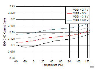
| Includes 1.57-mA sensor current | ||
| –40°C to +125°C |
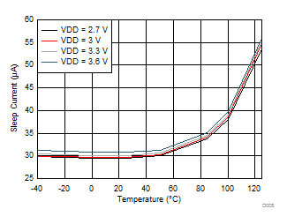
| –40°C to +125°C |
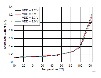
| –40°C to +125°C |
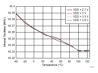
| –40°C to +125°C | ||
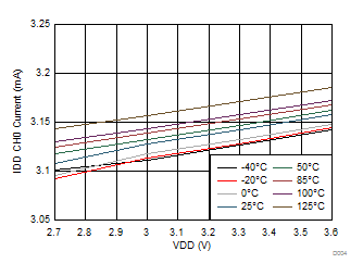
| Includes 1.57-mA sensor current | ||
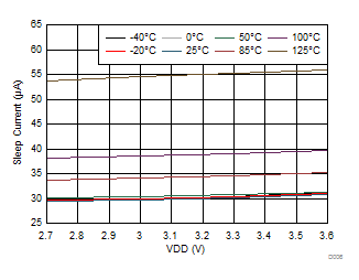
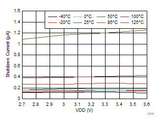
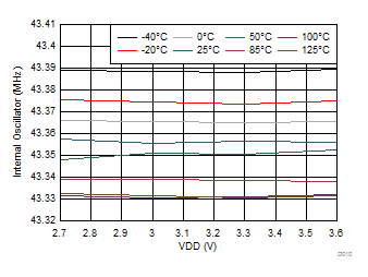
| Data based on 1 unit | ||